Silicon photonic integrated circuits made using wafer-scale technology
Over the last decade, silicon photonics has developed as an integration technology that supports a wide range of compact photonic devices on integrated circuits (ICs) for applications ranging from communications to sensing. Although the devices are technically interesting, silicon's greatest potential is as an integration platform for volume applications, leveraging huge prior investments. To realize this potential, we want to re-use the tools, processes, and knowledge that were developed for electronics to build photonic ICs. The specific requirements of submicron photonic integrated circuits, however, require new processes to support highly diverse optical structures. We have developed such processes in the last 10 years, based on mass-manufacturing, CMOS tools, including 193nm deep-UV lithography.
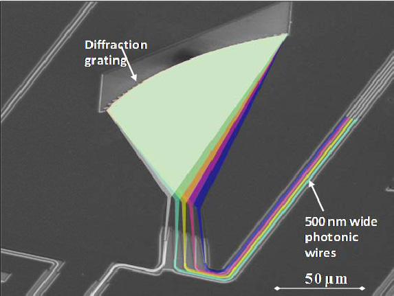
Silicon photonics now has low-loss, submicron wave-guides, strong optical confinement enabling extremely compact wavelength-scale components, and accurate, large-field processing. This large-scale integration allows for complex chips with high functionality, such as1,2 arrayed-waveguide-grating (AWG) and planar-grating devices for wavelength-division multiplexing (WDM) on footprints smaller than 0.1mm2, and channel selectors as small as 0.01mm2. A diffraction grating, acting as a part of an integrated spectrometer, is shown in Figure 1.

Silicon is not limited to communication devices, however. By influencing the on-chip light path with overlaid materials or chemistry, for instance in a microresonator, various types of sensors can be obtained, including label-free biosensors.3 The sensors are so compact that many hundreds or thousands can be integrated on a single chip.
While silicon is ideally suited for passive applications in the infrared, it is not a perfect material for active optics any more than it is for electronics. A major challenge is developing efficient light sources based on a silicon integration technology. Heterogeneous integration with III-V thin films may offer a cost-effective solution. Indium phosphide and gallium arsenide substrates can be bonded to the passive waveguide circuits in silicon-on-insulator, followed by substrate thinning and processing of thin-film lasers and detectors. A continuous-wave optical connection between microdisk lasers and microdetectors through submicron silicon waveguides, illustrated in Figure 2, was demonstrated in the Photonic Interconnect Layer on CMOS (PICMOS) research project,4 part of the Sixth Framework Programme for Research and Technological Development (FP6) of the European Commission (EC). Similarly, heterogeneous integration with other materials can bring new functionalities to silicon photonic ICs, such as all-optical signal processing based on strong nonlinear behavior in overlaid polymer materials.5
Driven by the European Network of Excellence on Photonic Integrated Components and Circuits (ePIXnet),6 the Interuniversity Microelectronics Center (IMEC, in Belgium) and the Electronics and Information Technology Laboratory of the French Atomic Energy Commission (CEA-LETI) have set up the Silicon Photonics Platform.7 This generic platform, with open design rules, gives external users with research and prototyping needs access to silicon-on-insulator technology. The cost to users is made affordable by extensive sharing of the mask and processing costs, using a multi-project-wafer approach. The prototyping service lets users obtain many samples for research on complex integrated circuits for various applications. The freedom in the processing is intentionally limited, so that standardization enables large freedom in circuit design. Access to the platform is open not only within the ePIXnet consortium but to the whole world.

The processes and devices currently offered include passive waveguides and photonic crystals in crystalline or amorphous silicon-on-insulator, silicon germanium epitaxy for active devices, and several standard modules such as fiber coupling. The platform users typically are involved in research on post-processing and packaging techniques, integration with III-V and polymer materials, research on new silicon photonic devices and applications for communications, optical signal processing, and sensing. This platform should help speed innovation in silicon photonics.
Pieter Dumon obtained a master's degree (2002) and PhD (2007) in electrical engineering from Ghent University. He now coordinates the ePIXnet silicon photonics platform, which gives access to the CMOS facilities at IMEC and CEA-LETI for wafer-scale research and prototyping of silicon photonic components.
Wim Bogaerts started in silicon photonics at Ghent University-IMEC in 1999. He developed CMOS-compatible processes for nanophotonic circuits, and obtained his PhD in 2004. He is currently a postdoctoral fellow of the Flemish Research Foundation, and member of IEEE-LEOS and OSA.
Roel Baets received a degree in electrical engineering from Ghent University, Belgium (1980), an MSc in electrical engineering from Stanford University (1981), and a PhD from Ghent University (1984). He leads the Photonics Research Group at Ghent University-INTEC (associated lab of IMEC), which focuses on new concepts for photonic components and circuits. Currently he coordinates the European Network of Excellence ePIXnet. Baets is a fellow of the IEEE.


