| #SPIElitho |

Students and others are encouraged to watch this webinar recording covering the basics of semiconductor lithography, the careers available, and a preview of Advanced Lithography + Patterning 2024. Opportunities for students to apply for full funding to attend the event in February is included in the discussion.
Watch to learn more!
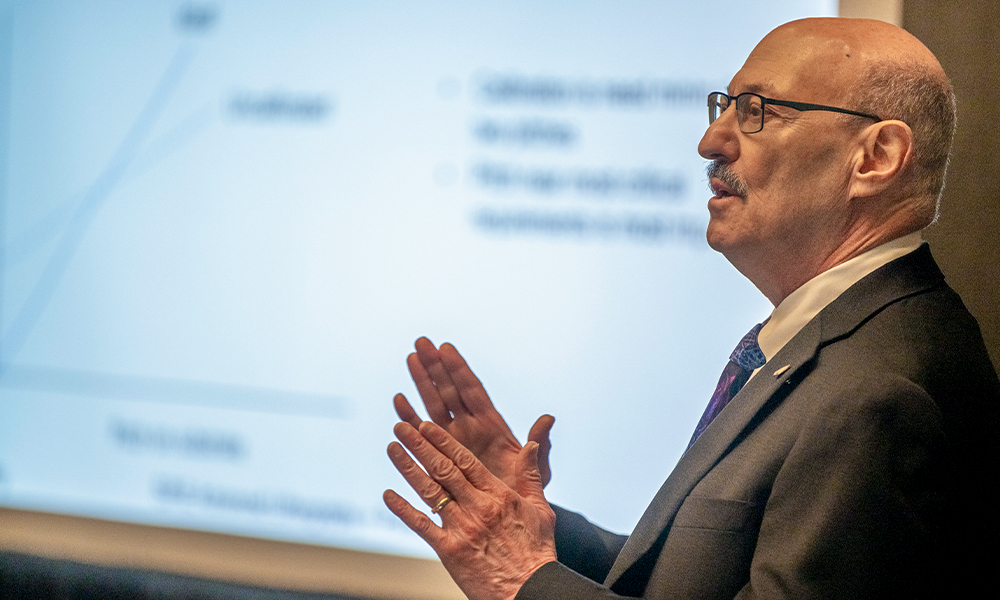
Advance your career and expand your skill set with instructional opportunities. Several courses will be available in San Jose.
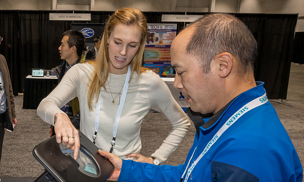
The exhibition at Advanced Lithography + Patterning is where people gather to collaborate and to get business done. Find these technology solutions and more:
• Photoresist, EUV, and other specialty materials
• E-beam lithography systems
• Precision cleaning, contamination, transport support materials
• Wafer treatments and substrates
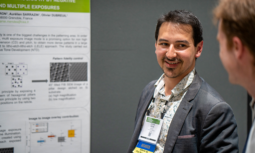
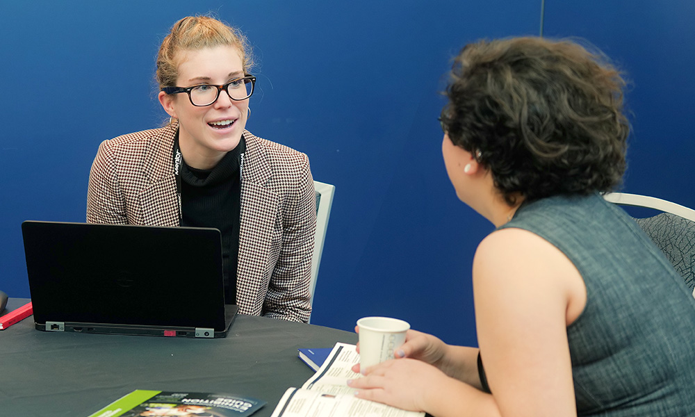
SPIE Advanced Lithography + Patterning offers numerous opportunities for students to engage and learn about the semiconductor industry, as well as share their latest research in lithography and photomask technologies. Leading companies support student participation through grants and awards, and tech groups offer scholarships for graduate and undergraduate applicants.
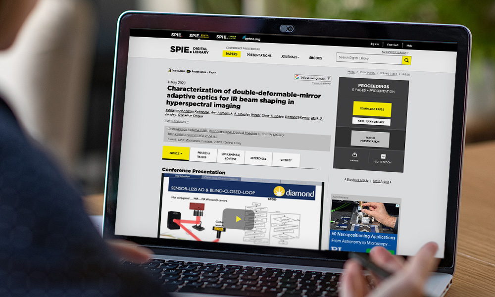
SPIE Advanced Lithography + Patterning conference proceedings are published in the SPIE Digital Library. All paid conference registrations include proceeding downloads with ongoing access through your SPIE account.
Visit the Digital Library to see all past years of proceedings from this meeting.