Highly selective dry-plasma-free chemical etch technique for advanced patterning
Currently, the areal scaling of central processing units continues in accordance with Moore's law for both the N7 and N5 (i.e., 7 and 5nm) semiconductor technology nodes.1, 2 To meet scaling targets and to maintain an aggressive gear ratio, however, achieving sub-30nm pitch line/space features at the back end of line (i.e., BEOL, the second stage of integrated-circuit fabrication where individual devices are interconnected with wiring on the wafer) is key. A number of patterning strategies enable the fabrication of such small features: extreme-UV (EUV) direct print; 193nm immersion-based self-aligned quadruple patterning, SAQP; 193nm immersion-based lithographic etch, (LE)x; and directed self-assembly, DSA. Source power concerns preclude EUV direct print, and overlay and line-placement roughness (LPR) preclude 193nm immersion-based (LE)x and DSA, respectively.3, 4 The only technique that is ready for high-volume-manufacture (HVM) applications is the 193nm immersion-based SAQP.5, 6
 Although SAQP has been successfully implemented at the front end of line (FEOL, where individual devices are patterned onto the semiconductor) since the development of the N10 node, the technique is new to BEOL, and brings with it a different set of challenges. One such challenge is the limited choice of materials that can be used as films because of the lower temperature budget (i.e., below 400°C). The films that can be deposited at such low temperatures are generally of poor quality compared to their analogous high-temperature versions because of differences in, for example, crystallinity and composition. Because of these characteristics, conventional plasma-etch techniques often have less than the required etch selectivity. This causes significant gouging (i.e., unintended etching of the etch-stop layer) and line-edge roughness and line-width roughness (LER/LWR), which may result in poor uniformity and pitch walk (i.e., variation in pitch) at downstream processes.
To improve the etch selectivity for certain etch steps during the SAQP flow, we have developed a highly selective, plasma-free, chemical gas-phase etch technique. Our approach uses chemistries that have high selectivity toward a range of films, owing to the reaction mechanism. Gas-phase etches also help to eliminate plasma damage to the features (i.e., corner rounding) during the etch process. Our technique has the potential to improve SAQP process performance for BEOL-compliant films, and could also enable profile improvement, selective mandrel pull, and critical dimension trim of the mandrel profile (to meet the desired height and width).
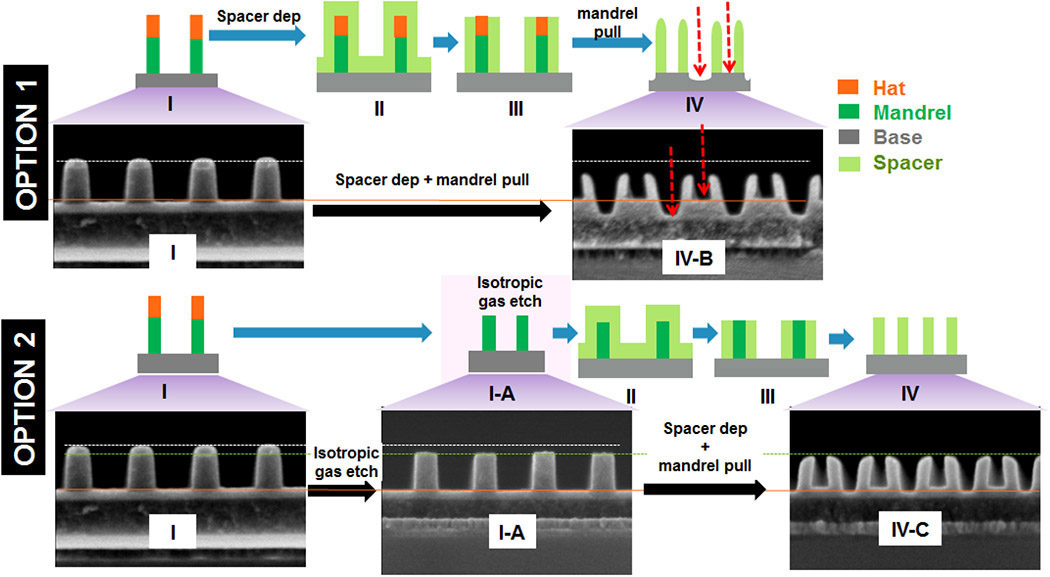
A typical SAQP process involves two sequential self-aligned double-patterning (SADP) steps, with the help of two mandrels at each SADP level: see Figure 1.6 The first mandrel definition is obtained by an all-in-one dielectric antireflective coating (DARC) etch and mandrel etch.6 Figure 1 shows two options at this first mandrel to achieve the first set of SADP structures. The first option involves spacer wrap around the mandrel and DARC, followed by an all-in-one spacer etch-back and mandrel pull by plasma etch. The lack of plasma-etch selectivity between the hat and mandrel materials, with respect to the base, causes gouging at the base of the structure (i.e., the etch-stop layer). This creates an asymmetric profile between the mandrel side and the spacer side, as highlighted with red arrows in Figure 1(IV). During subsequent processes, this asymmetric profile may lead to poor local critical dimension uniformity, LPR, LER, and LWR. Such variations in the patterned features can cause significant edge-placement error (EPE).7 By implementing an additional mandrel/profile improvement step, however—see Figure 1, option 2—we were able to mitigate the pattern asymmetricity post spacer etch-back mandrel pull (SEMP).

In the first step, we employed mandrel/profile improvement. This step involves a highly selective gas phase etch of the ‘hat’ material—e.g., silicon oxynitride, silicon dioxide (SiO2), or silicon nitride (Si3N4)—thus leaving a square-shaped mandrel. We achieve extreme etch selectivity by carefully choosing the gas mixtures and other process parameters (e.g., pressure and temperature). Additionally, due to the plasma-free nature of our technique, plasma damage to the spacer profiles during etch is entirely avoided. Profile improvements between the two final structures—see Figure 1 IV-B and IV-C—are therefore primarily achieved by eliminating the DARC etch during the all-in-one plasma SEMP step, thereby providing a better process window and lowering the etch-selectivity criteria during the plasma SEMP step. Furthermore, we observed that the selective removal of DARC contributes to an improvement of ∼10% in LER and ∼30% in LWR.
The second patterning application for our plasma-free etch technique relates to mandrel pull. We have shown that a gas-phase etch enables superior SAQP flow with fewer process steps and better performance.6 In this case we have shown that by changing the etch chemistry, we are able to selectively etch amorphous silicon (a-Si) mandrel material with >100:1 selectivity to SiO2 and Si3N4, as shown in Figure 2. Depending on the patterning stack, by carefully selecting the gas combination, we can modulate the etch selectivity between alternate material choices. This high selectivity is a direct manifestation of the chemistries that we implemented during etches. Significant improvements can be seen in terms of gouging and spacer shape in the gas-phase mandrel-pull results—see Figure 2(a)—compared to the plasma-assisted a-Si etch: see Figure 2(b). These have been shown to improve LCDU (local critical dimension uniformity), LPR, LER, LWR, and downstream pitch walk, which may further minimize EPE issues.7

In summary, we have developed a non-plasma-based etch technique for SAQP and multi-patterning schemes. The selectivity of gas-phase etches represents one of the key advantages of our technique. This high selectivity is primarily due to the reaction rate and reaction/etch mechanism specific to the film compositions. The reaction rate can further be controlled by tuning the process parameters and gas ratios, and the reaction mechanism can be controlled by carefully choosing the gas/etchant mixtures and gas concentrations. We are currently investigating the reaction pathways and mechanisms that enable such plasma-free etch techniques, and are further exploring new chemistries and techniques to etch new materials.
Subhadeep Kal is a process engineer at Tokyo Electron America, where he works on a variety of multi-patterning schemes and alternate integration schemes for logic and memory applications. He is particularly interested in nanoscale R&D fabrication for advanced electronic devices.


