A spacer-on-spacer scheme for self-aligned multiple patterning and integration
To enable lithographic printing of ever smaller features, multipatterning techniques are increasingly being used in the semiconductor industry. These techniques are designed to extend 193nm immersion lithography, which is necessary to enable designs at 20nm or below. Multipatterning methods, however, are typically two to three times more expensive for each wafer than for a theoretical 193nm-immersion-based single exposure (assuming that 193nm immersion could be used to achieve the desired pitch). Moreover, extreme UV (EUV) lithography—a technology for the 5nm node that is expected to be available after 2020—is a costly option for high-volume production at major foundries and integrated device manufacturers (see Figure 1).1

At present, self-aligned quadruple patterning (SAQP) is the optimum technique for patterning of layers that require the most aggressive pitch shrink (such as fin formation and critical metal layers). In a standard SAQP stack, two hard mandrels are used alongside the appropriate etch stop and hardmask layers (see Figure 2). Integration of these components, however, is complex and involves several sacrificial layers that require multiple dry-etch and wet-etch steps. In response to this complexity, developers have so far made several attempts to simplify multipatterning processes, and to reduce costs and improve throughput.2, 3

We propose a low-cost alternative SAQP scheme that features no sacrificial layers, and which uses a spacer-on-spacer pitch-splitting strategy (see Figure 3). With our method, which requires careful selection of the underlying substrate, mandrel, and spacer materials, we can achieve a 25% reduction in cost compared with the traditional SAQP approach. In our demonstration of this technique, we took an atomic layer deposition (ALD) film material—which we used for the first spacer (spacer 1)—and successfully used it as a second mandrel. We achieved this by optimizing the spacer shape to minimize the second spacer (spacer 2) mask asymmetry, which could otherwise cause line-edge roughness (LER) degradation and could have a significant impact on the edge-placement error during the final pattern transfer. When defining the first mandrel pattern, it was necessary to select the etch process according to the underlying layer, i.e., so that it caused minimal gouging. For the same reason, we had to consider the substrate when selecting the chemistry of the spacer 1 and spacer 2 etches. After completing the spacer 2 etch, we thus removed the spacer 1 etch selectively to the spacer 2 material and to the substrate.
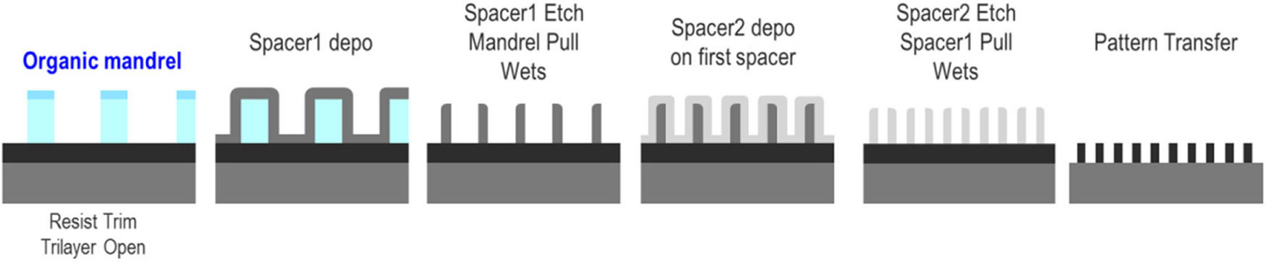
By meeting all the selectivity requirements, we demonstrated that our scheme has a superior process performance and control of pitch walking (where mask misalignment causes anomalies in the pitch) than the SAQP approach. No pattern was transferred to the underlayers (except at the last step), therefore there was minimal variation in the critical dimensions (CDs) through pattern transfer to the underlying masks. In addition, by using the ALD spacer films, we were able to further control CD variation. We used the organic litho stack material as a first mandrel, and an ALD room-temperature silicon dioxide film (which is compatible with organic materials) as a first spacer. We used a low-temperature titanium dioxide ALD film as a second spacer, and titanium as the underlying substrate for patterning.
Our scheme has a low thermal budget, and can thus easily be implemented at the ‘back end of line’ (the second stage in integrated circuit fabrication). We conducted all anisotropic etches in a capacitively coupled plasma chamber with a high-frequency power source on the top electrode and a low-frequency source on the bottom electrode. This chamber configuration enables independent control of plasma density and ion energy. We used a plasma-free gas-phase etch process tool to remove dielectric antireflective coating (DARC) and to remove spacer 1 (selective to spacer 2 and the underlayer). This tool can be used to remove both materials (DARC and silicon dioxide) with minimum damage to the underlayer and the spacer 2 mask. During this process, we introduced gases on the wafer, where they adsorbed and formed a finite layer of modified material. We then heated the wafer to sublimate the modified layer, and repeated this isotropic process in cycles until we had removed the desired amount of material. In this way, we achieved a high-selectivity, damage-free controlled etch. It is also possible to modify the gases that are used to remove various target film materials.
Our integration concept is illustrated in Figure 4 on silicon, from mandrel patterning (left) to final pattern transfer (right). In addition to cost and throughput concerns, line-width roughness (LWR) and LER are important parameters for process-performance benchmarking since they affect device performance directly.4 We compared the spacer-on-spacer SAQP pitch-splitting process performance, in terms of LER/LWR, against previously demonstrated flows,5 and found that the two were equivalent. We can execute our spacer-on-spacer integration with various permutations of the ALD spacer and mandrel materials to suit the needs of each application. In addition, it may be possible to achieve more aggressive scaling down (to 20nm pitch) without experiencing the problems of high aspect-ratio line wiggling, since all patterning is executed on the same level.

In summary, we have demonstrated a spacer-on-spacer pitch-splitting SAQP integration that reduces the processing costs of standard integrations. Our method enables patterning of sub-30nm pitch applications (e.g., fins and critical layers), and—thanks to the reduced number of processing steps—it shows great potential for cost savings and throughput improvements. The key challenges that remain are the selection of appropriate materials to guarantee adequate selectivity, and engineering of the spacer shape to prevent edge-alignment errors. Our future aim is to demonstrate the feasibility of our technique at lower pitches and to explore additional material sets.
Angélique Raley is a senior process engineer whose research focus is on plasma etch development for advanced technology node patterning.


