A 40-year roadmap

In a plenary presentation that opened the 2024 SPIE Advanced Lithography + Patterning conference, Todd Younkin said that the goals of the semiconductor industry must shift. That new direction means that the focus of research and development will have to change. It’s all part of what he predicted will be a long running trend.
"We're entering the next 40-year era of semiconductor innovation. And that’s not based on fastest, cheapest, smallest, throw-it-away [electronics] but on the practical, energy efficient use and consumption of electronics,” said Younkin, president and CEO of SRC, an organization that funds a global semiconductor research agenda.
Younkin noted that in supporting the semiconductor industry, lithography and patterning have achieved notable successes. For example, extreme ultraviolet, or EUV lithography, has moved into high-volume manufacturing, showing up in such consumer devices as the latest smartphones. EUV should eventually lead to a 40 percent shrink in device feature sizes and 3x improvement in transistor density. Advances planned for the technology over the rest of the decade promise to keep it on track to deliver the needed manufacturing capabilities.
However, even though EUV has a bright future Younkin noted the semiconductor industry it supports faces three fundamental challenges: prosperity, people, and the planet. Solving these issues will require a threefold increase in investment in critical research areas, a tripling of the size of the workforce, and a focus on sustainability.
Regarding the last two items, the average age of people working in semiconductors is 57, Younkin said. Getting the next generation of innovators interested in solving semiconductor challenges requires having them work on important and worthwhile issues, like saving the planet.
Improving sustainability of chip manufacturing and use addresses this need as well as solving a looming industry roadblock. The energy devoted to computing and communication is exploding, driven by such innovations as the rising use of artificial intelligence (AI). Energy use is also growing because of activities such as the sharing of cute cat videos, Younkin noted.
Estimates are that over the next few decades there needs to be as many as six orders of magnitude improvement in chip manufacturing and device-use energy efficiency. Younkin said there has already been about a hundred-fold, or two orders of magnitude, improvement in chip manufacturing energy efficiency. If that progress fails to continue, then computation and communication will eventually be a significant and therefore unsustainable share of worldwide energy usage.
“It’s a holistic problem,” Younkin said.
The solution, he argued in his presentation, must also be holistic. Much of such a total answer involves packaging, the final stage of semiconductor manufacturing. During packaging, manufacturers encapsulate a semiconductor die in a supporting case that prevents physical damage and corrosion while allowing electrical connection to the outside world.
Part of the packaging advancement needed involves 3DHI, or three-dimensional heterogeneous integration. Having this capability would allow manufacturers to use the best possible combination of chip materials and manufacturing techniques. As a result, they could produce a device that is as energy efficient and environmentally friendly as possible.
Advanced lithography has traditionally focused on the smallest possible features and thus the tiniest length scales, which today measure nanometers. There is a need, though, for those who push lithography limits to look at all length scales, from nanometers, or billionths of a meter, to kilometers, or thousands of meters, Younkin said.
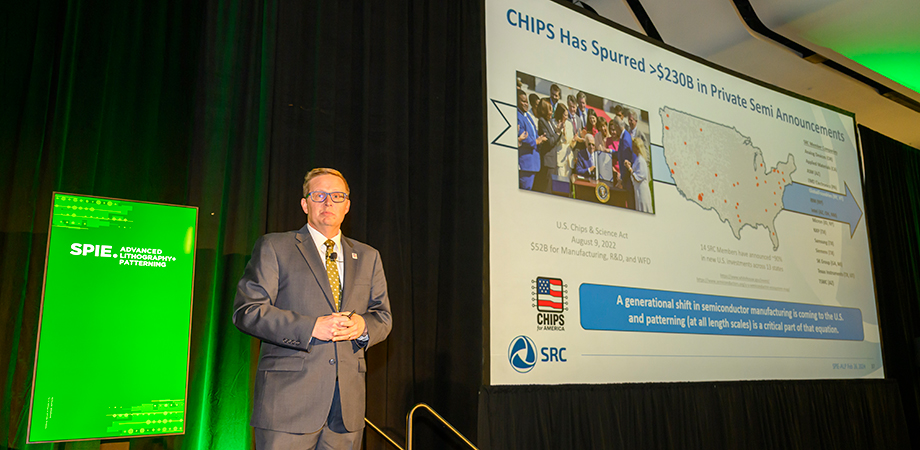
As he started to wrap up his presentation, Younkin stated that the pace of progress in meeting these challenges could accelerate due to the 2022 passage of the CHIPS and Science Act. It is part of a worldwide trend of investment in semiconductor technology. A significant part of the CHIPS Act funding aims to expand the workforce, with the goal of ensuring a large enough pool of skilled personnel.
In summarizing his talk and issuing a call to action, Younkin noted challenges and pointed to opportunities. Together, they point to a future that he finds bright.
As he said, “There has never been a better time to be a part of the semiconductor industry and this patterning community.”
Hank Hogan is a science writer based in Reno, Nevada.
| Enjoy this article? Get similar news in your inbox |
|


