Photonic device fabrication using ultrafast laser waveguide inscription
Lightwave circuits (LCs) are the optical equivalent of electronic integrated circuits. However, instead of using thin metallic wires to control the flow of current, LCs use the principle of total internal reflection to guide light along micron-scale dielectric wave\-guides. Using such waveguides, complex optical circuits can be constructed to perform multiple functions on an input optical signal.
Currently, most LCs are fabricated using approaches that rely on photolithography to define the waveguide regions. Such techniques are expensive for device prototyping and do not lend themselves to 3D device fabrication. Recently, a new fabrication route using ultrafast lasers has attracted significant interest. By focusing femto- and picosecond pulses of sub-bandgap radiation inside a dielectric material, optical energy can be deposited in the focal region by nonlinear absorption. The deposited energy can modify the refractive index of the material at the focus, which can then be used to fabricate optical waveguides. This is done by translating the material in three dimensions through the focus, as shown in Figure 1.

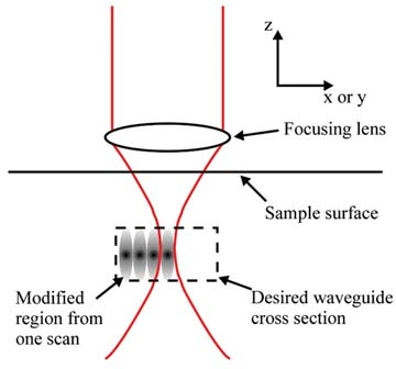
Our efforts in this field are directed at fabricating broadband optical amplifiers and nonlinear optical devices. In our optical amplifier work, we have fabricated waveguides in two types of active glass: Bi-doped silicate1 and Er-doped oxyfluoride-silicate,2 both supplied by Animesh Jha's group at the University of Leeds. To fabricate these waveguides, we have used the recently demonstrated ‘multiscan’ fabrication technique to control the waveguide cross-section and the refractive index contrast independently.3 The multiscan technique uses many successive scans of the sample through the focus to construct the desired waveguide cross-section from the individual lines of the modified material created by each scan, as illustrated in Figure 2.
Our Bi-doped glass work demonstrated the successful fabrication of low-insertion-loss waveguides and—significantly—ultra-broadband fluorescence emission with an FWHM (full-width half-maximum) of over 500nm centered at 1.3μm under optical pumping.1 An optical amplifier that shows such a large bandwidth in the 1.3μm region has great potential for telecommunications applications. Experiments are under way to characterize the gain operation of these waveguides.
As a result of our Er-doped glass work, we demonstrated, for the first time, internal gain from an Er-doped oxyfluoride-silicate glass waveguide.2 Figure 3(a) shows a micrograph image of the multiscan fabricated waveguide facet after polishing. Figure 3 also compares the near-field images of the 1550nm mode obtained from the fabricated waveguide (b) and from a Corning SMF-28 fiber (c). The waveguide cross-section is close to symmetric, exhibiting a 1550nm mode comparable to that of the SMF-28 fiber. Figure 4 shows a photograph of the bidirectionally pumped Er-doped waveguide. The homogeneity of the green upconversion confirms the low-loss nature of this waveguide. We are confident that further device optimization will yield substantial net gains comparable with those reported using phosphate glass hosts.


Through our optical modulator and wavelength converter work, we have also demonstrated a waveguide fabricated in crystalline LiNbO3 using ultrafast laser waveguide inscription that supports a well-confined mode at 1550nm.3 We believe that this result could pave the way to fabricating novel nonlinear devices and modulators for telecommunications applications.
The potential of ultrafast laser waveguide inscription to fabricate already existing as well as entirely new 2D/3D photonic devices is clearly very high. It is our belief that this technique has only just begun to be seriously explored and that the next few years will represent an extremely fruitful and exciting period of investigation.
Robert Thompson received his BS (with first-class honors) in physics from Heriot-Watt University in 2000, his MS in optoelectronics and laser devices from the University of St. Andrews in 2001, and his PhD from Heriot-Watt University in 2006. His current research interests are centered on the fabrication of photonic devices using femtosecond lasers.
Henry Bookey received his BS (Hons) in physics and astronomy from the University of Leeds in 1997 and his MS and PhD from Heriot-Watt University in 1998 and 2004, respectively. His current research interests are centered on chalcogenide glasses for ultrafast optical switching and Er-doped waveguide amplifiers for telecommunications applications.
Nicholas Psaila received his BSc (Hons) in physics from Imperial College London in 2003, and his MS in photonics and optoelectronic devices from Heriot-Watt and St. Andrews Universities in 2004. After a short spell in industry, he is now working toward completing a PhD. His research is primarily concerned with femtosecond laser waveguide inscription.
Ajoy Kar received his MS from Delhi University, India, in 1973 and his MS and PhD from the University of Essex in 1975 and 1978, respectively.His current research interests involve amplifiers for telecommunications, ultrafast all-optical switching in novel optical fibers, and generation and propagation of white light continua through the atmosphere for LIDAR (light detection and ranging) applications.


