Single-digit nanometer nanoimprint templates
Shrinking the size of transistors on a chip makes it possible to integrate more functions in a device, and achievements in micro/nanolithography have enabled an exponential growth process, known as Moore's law, that has guided the semiconductor industry for more than four decades. Continuing this, however, demands integrated circuits at sub-10nm sizes within the decade.
A candidate technology for fabricating such integrated circuits is nanoimprint lithography (NIL).1 Using randomly dispersed single-wall carbon nanotubes as a template, it offers a resolution of 2nm.2 In addition, NIL has a unique ability to pattern nanostructures on large non-planar surfaces at high throughput and low cost, which is particularly important to many emerging applications, such as energy conversion, biomedical sensing, and data storage.
NIL's power relies on the master template carrying the high-resolution nanostructures, which typically have been created by electron beam lithography (EBL). However, in a sub-10nm regime, conventional EBL suffers from a significant proximity effect—that is, the negative effect on nanopatterning by a nearby nanostructure—rendering the patterning of arbitrary dense structures on a large area very challenging. A number of other factors also limit further improvement of EBL resolution, including the resist development process, spot size (which is limited by electron diffraction and aberrations in the system), and broadening of the primary beam by electrons generated in the resist material (secondary electron broadening).3


A recently introduced technique, helium ion beam lithography (HIBL),4,5 may hold the key to further pushing the frontiers of sub-10nm nanolithography patterning. In a helium ion microscope (HIM), helium ions from a high-brightness source are focused at a small spot size and scanned over the sample for imaging with a record high resolution of 0.24nm. When used in lithography applications, the focused helium ion beam is superior in several ways to conventional EBL. As well as high resolution, it has a negligible proximity effect, and a wide ‘process window’ (i.e., exposure range), thus making it a promising tool for creating sub-10nm arbitrary patterns on nanoimprint templates. Duplicating sub-10nm HIBL-defined patterns by NIL combines the merits of high throughput and low cost, and is therefore an ideal solution to HIBL's intrinsic problem (as a serial patterning method) of high cost and slow writing speed.
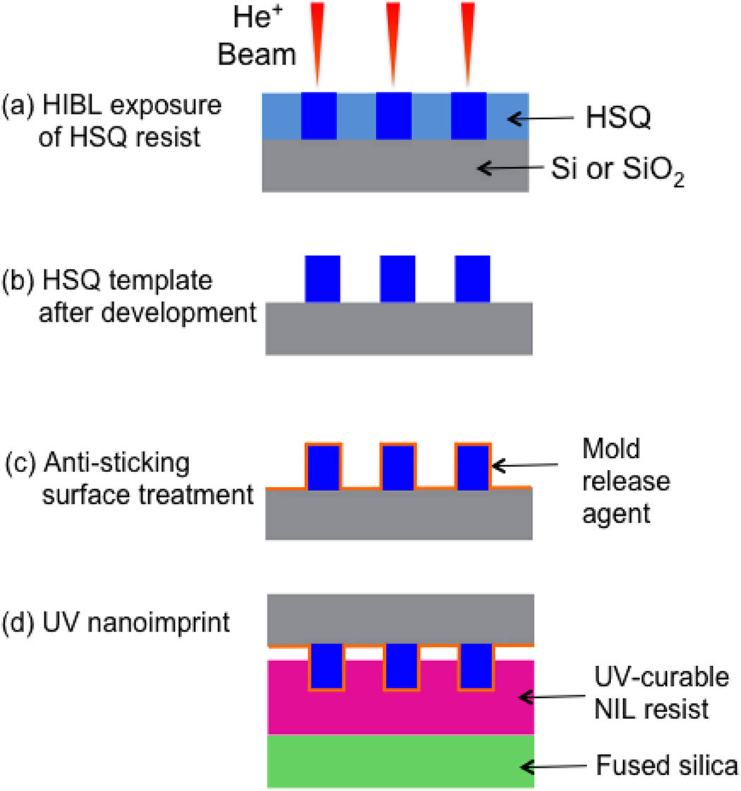
We recently demonstrated this combined helium ion beam and nanoimprint lithography,6 following a procedure outlined in Figure 1. We first performed HIBL using a Carl Zeiss Orion Plus scanning HIM equipped with a Raith ELPHY MultiBeam pattern generator on a 12nm-thick hydrogen silsesquioxane (HSQ) resist spin-coated on a silicon substrate: see Figure 1(a, b). The HSQ resist not only provides high resolution in HIBL patterning but also exhibits high mechanical strength after crosslinking so that it can be used directly as a nanoimprint template. Using crosslinked HSQ as the template eliminates the transfer of sub-10nm patterns into other hard template materials and avoids loss of pattern resolution and accuracy during the transfer process. An anti-sticking surface treatment of the HSQ template completes its fabrication: see Figure 1(c). A standard UV-curable nanoimprint process on a transparent glass substrate was subsequently followed to transfer the sub-10nm patterns on the template to the nanoimprint resist: see Figure 1(d).
Using this combined approach, we successfully patterned 4nm half-pitch lines in HSQ using HIBL and transferred this pattern into a resist layer through NIL: see Figure 2. Our result of 4nm half-pitch lines patterned by HIBL in HSQ provides the experimental evidence that HIBL can achieve a patterning resolution comparable to or even higher than that achieved by EBL, which was expected but has not previously been demonstrated. The nanoimprinted 4nm half-pitch line pattern is also the smallest designed pattern obtained by NIL to date.
In addition to the record high resolution, we have also shown that the negligible proximity effect and wide process window of HIBL, which are both attributed to a reduced ratio of backscattered helium ions compared with that of backscattered electrons in conventional EBL, can benefit the fabrication of NIL templates. This is particularly desirable when making nanoimprint templates containing dense and complex nanoscale patterns, and the wide process dose window reduces the sensitivity of template pattern accuracy to the exposure dose variation.
In summary, we have experimentally demonstrated a combined helium ion beam and nanoimprint lithography method and achieved 4nm half-pitch lines patterned by HIBL and transferred by NIL. This approach combines the advantages of HIBL (high resolution, low proximity effect, and wide process window) with NIL's low cost and high throughput, and is a promising fabrication tool for sub-10nm devices. We are currently working to improve the durability of the single-digit-nanometer nanoimprint template. To increase the lifetime of the template, we need to study and optimize the mechanical properties of the template materials at this unprecedented scale. Moreover, we are also further developing post-lithography processing steps, such as etching and material deposition.
Hewlett-Packard Company
