Staking a claim on the next best thing since glass: Entrepreneurs and the metalens moment
The “Seated Scribe,” a statue depicting an important servant who would be needed for the journey to the afterlife by some high-caste person in ancient Egypt’s Fourth Dynasty, today sits on exhibit in Paris’ Louvre Museum. Gazing outward, forever writing on a roll of papyrus spread across his lap, the sculpture looks as it did upon entombment beneath the Sahara desert some 4,500 years ago.
But what is most striking about the statue are the Scribe’s eyes. They are primitive lenses, carved from clear quartz and then assembled with other materials to replicate the look of the human eye, including coloration, an iris, and a pupil. This and similar statues from ancient Egypt are often so lifelike that the eyes appear to follow onlookers as they move around it.
The Scribe’s eyes demonstrate how ancient Egyptian technology, funerary arts, and knowledge of human anatomy came together long ago to give the world one of the first transparent lenses created to produce an optical effect. The first known mirrors—shaped and polished pieces of obsidian—date back even further in human history to some 8,000 years ago.
Today, of course, glass lenses are ubiquitous and vitally important for tasks like scanning documents or taking selfies with a smartphone; imaging the universe with advanced optical glass and mirrors in giant telescopes; or using delicate, miniature camera lenses that see inside the body to deliver advanced healthcare.
The glass optics industry, expected to reach a world market value north of $25 billion by 2028, relies on armies of highly trained professionals using advanced software and hardware to produce the optical components with which we see all that can be seen, and then some.
But a new revolution in lens making is underway—maybe the next best thing since glass. It is the metalens, comprised of nanostructures or nanofins arranged on a surface capable of capturing images at subwavelength resolution, and with quality comparable to state-of-the-art commercial objectives.
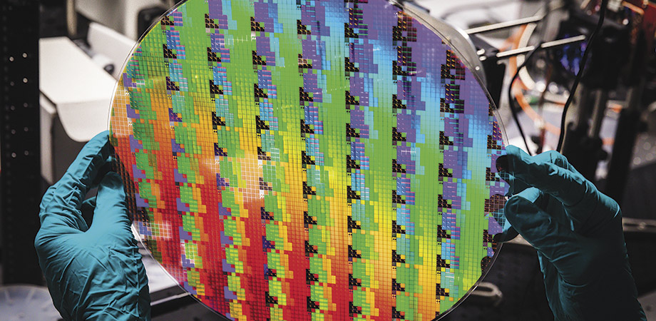
An important part of the revolution is that metalenses can be mass-produced, etched onto a substrate using deep ultraviolet lithography—the same processes used to fabricate advanced semiconductor chips. This scalability is crucial, especially for applications in consumer electronics where form factor, cost, and the ability to manufacture millions of devices very quickly is a make-or-break part of the business.
Metalens entrepreneurs see the potential and are trying to deliver these disruptive lens technologies to market. On the near horizon, they anticipate cell phones with unparalleled facial recognition and picture-taking capabilities, all within a form factor about the size of a credit card; sensors that can capture light polarization information for unprecedented depth perception and even the molecular makeup of objects; and endoscopic cameras so tiny and thin they can be threaded into human bronchial tubes where they might detect lung cancer at an early stage when aggressive treatment can save lives.
As first described by Harvard University’s Federico Capasso and colleagues in 2016, metasurfaces are “subwavelength-spaced phase shifters at an interface that allow for unprecedented control over the properties of light.”
Capasso is considered the pioneer of metasurface science and technology, which he describes primarily as a breakthrough based on the understanding of how light beams can be shaped in a nearly arbitrary way using Fermat’s principle to minimize light’s optical path. In conventional optics, he explains, gradual phase shifts accumulated during light propagation are used to shape the wavefront of light beams, for example, to focus light. But this is done using thick and bulky materials—like glass.
But by introducing phase changes over a subwavelength scale along the optical path, he realized, new degrees of freedom in shaping light can be attained. To do so, his group experimented with different methods of imprinting such phase shifts on light beams: arrays of optically thin metallic antennas to redirect light, followed in 2016 by the first high-
performance metalens with then-graduate student Robert C. Devlin—who developed metasurfaces of TiO2 nanofins defined by lithography and atomic layer deposition—and postdoctoral fellow Reza Khorasaninejad. Operating in the visible, they demonstrated focusing performance comparable to state-of-the-art complex and bulky microscope objectives.
Should optical glassmakers be nervous?
“To some extent, yes,” says Devlin, who is now CEO of Boston-based Metalenz, a company he co-founded with Capasso that holds some 20 patents on metasurface technologies. “I mean, there are areas where metasurfaces are going to displace conventional lenses, conventional optics. But we’re also moving this into foundries, right? That’s the other piece. It’s not just that we have a new lens, it’s where the lenses are going to be manufactured.”
He continues, “I think it would be a little bit too much to say that there are never going to be places for glass lenses that have been around since Egyptian times. There are a lot of places where metasurfaces provide substantial advantages. Glass lenses and plastic lenses—you know, conventional molded refractive lenses—will still have some advantages. But over time, metasurfaces and what we’re doing at Metalenz will take more and more of that market share.”
Last June, Metalenz announced that its planar metasurface optics are being manufactured in STMicroelectronic’s (ST) semiconductor fabs—the first metasurface technology to become commercially available. “The metaoptics collect more light, provide multiple functions in a single layer, and enable new forms of sensing in smartphones and other devices, while taking up less space,” ST said in announcing the deal.
Prior to working with Metalenz, ST made a more conventional sensor device module using refractive and diffractive lenses. “They’re adding Metalenz technology to their modules,” Devlin says. “[The previous sensors] have been in something like 200 smartphone models, as well as laptops and other applications. It’s a whole gamut of optical devices that consumers have interacted with. They’ve sold more than two billion units of that [historic] device. So, it’s quite a large volume that will be impacting consumers directly with our metasurfaces.”
At Canadian firm META (Meta Materials Inc., no relation to the company sporting the big blue thumb), improving 5G broadband communications is just one near-term application of its metasurface technology enhanced by artificial intelligence software design tools for customized applications. While their products are not aimed at replacing glass, they place metasurfaces on transparent films that can move optical or radio frequencies in highly controllable ways that can radically enhance the functionality of glass and other surfaces.

A scanning electron microscope image of META’s metalens, made using electron beam lithography and dry etching techniques. Photo credit: META
Back to smartphones, for example.
“5G signals are notoriously bad at propagating and penetrating both outdoors and especially indoors,” says META’s Rob Stone. “Because [the signals] are higher frequency, they can carry more data. That’s the promise of 5G: broadband speeds, wirelessly. But the signal has a shorter range, and if it encounters an object in the environment, it’s very easily absorbed or attenuated.”
But with the company’s NANOWEB transparent conductive film, he says, “we can take the signal that starts on a cell tower, up above a building somewhere, and bounce it off the side of a building across the street. Since it’s transparent, we can put it on the windows, and guide that signal down to the shadow of the first building, where the 5G signal no longer reaches, and fill in dead spots on the street.”
Inside a building, Stone continues, the film can control the angle of reflection to take a signal that’s going down a hallway and make it bend around the corner, down the hall, and into a conference room. “And this is all passive. It’s a transparent plastic film so it can go over the architecture without disturbing it. You can paint over it. No wiring, no power required.”
The same platform can be used for transparent heaters on advanced driver-assist systems. “The lidars and radars on the high-end new cars that give you wonderful safety features—you know, auto cruise control and semi-self-driving—all of that is of no use if there’s a little bit of fog or ice and snow and the sensor window gets blocked.” META’s NANOWEB platform, on the other hand, can provide transparent heating and EMI shielding that does not disturb either the lidar or radar. The technology can de-ice or de-fog an entire windshield or sunroof of a car.
“We can apply electrochromic technology to shade the sunroof to the desired transparency, and we can embed 5G antennas into the glass that do not spoil the view—all invisible to the human eye,” Stone says.
The secret to commercial success for META will also be its scalable manufacturing technology—roll-to-roll production of transparent films that maintains the integrity of the nanostructure waveguides that combine high conductance with high transparency.
For other startups, the approach is to use new surfaces—meta or not—to design an innovative optical system that can’t be achieved using refractive lenses. For example, medical-device company LeadOptik is building a fiber-thin 3D imaging probe for minimally invasive detection of lung cancer using advanced diffractive optics. Like metalenses, these are flat optics that rely on surface features to shape beams of light in desired ways for desired outcomes.

LeadOptik assembles several flat optical components on the tip of a fiber to create a 3D medical imaging probe. Photo credit: LeadOptik
LeadOptik’s goal has been to leverage whatever has been done in refractive optics and combine it with advanced diffractive optics to include some of the magic of metasurfaces. Most important are the flat optical components: “We can build an adaptive focusing technology in submillimeter form factor,” founder and CEO Khorasaninejad says. “This core technology enables a world-first, multifocal 3D imaging probe that can reach and perform high-resolution imaging anywhere in the lung.”
Why does size matter? First, in most cases, lung cancer starts from the periphery of the lung where airways are very small in diameter and hard to reach by any other technology. “Second, every time you want to integrate an imaging probe with a surgical device you always want the imaging probe to take less space,” Khorasaninejad says. “You don’t want to interfere with the mechanical part of your surgical device.”
In the case of LeadOptik’s 3D imaging probes, which are like tiny zoomable microscopes on the tip of an optical fiber, the goal is to navigate passageways through the human lungs and be able to locate cancer lesions and measure depth information—for example, allocation (relative to the airway) and size of cancerous lesion—with a high degree of accuracy.
That depth is critical information for a surgeon, who would want to remove enough diseased tissue that the cancer does not return. The information is even more critical if the cancer in question is occurring in the brain. But the company’s focus, for now, is giving doctors a tool to better diagnose lung cancer, which is three times more deadly than the next deadliest cancers combined.
Khorasaninejad says there are lots of potential applications for LeadOptik’s medical imaging technology, including to diagnose other types of cancer. But for a young company trying to win FDA approval for a new device, he says, “we really need to do just one thing right.”
For startups like Metalenz, LeadOptik, and more, the venture- capital funding and interest from large corporations they are attracting would suggest the metalens magic is working. Glass or no glass, our devices can seemingly never be small enough or have enough functionality to satisfy the marketplace. But a thousand years hence, it’s worth considering that the humble Seated Scribe and his rock-crystal eyeballs will most likely still be following our every move.
William G. Schulz is Managing Editor of Photonics Focus.


