US President Joe Biden signs historic CHIPS and Science Act
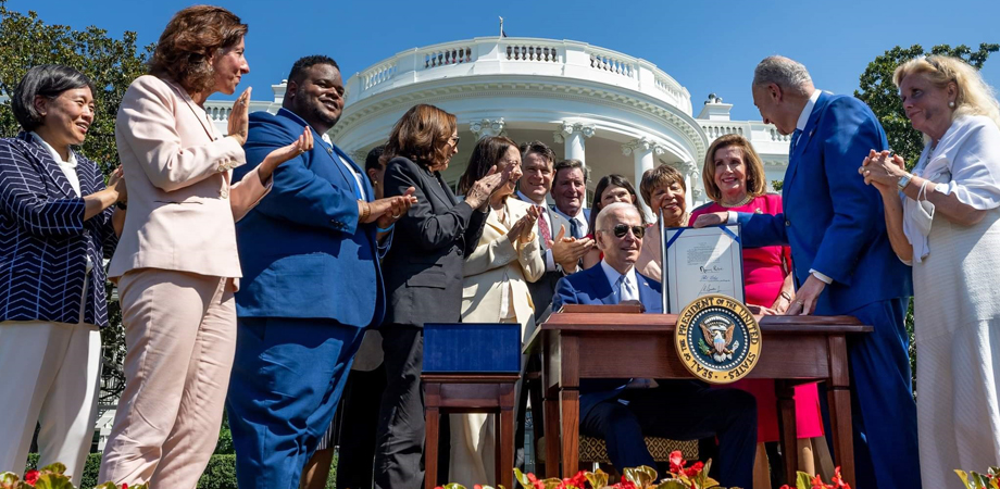
At a White House ceremony, US President Joe Biden today signed the historic CHIPS and Science Act of 2022, unleashing historic investments in research, development, and infrastructure aimed at building a more robust domestic semiconductor manufacturing capacity.
In a statement, the White House said the new law “will strengthen American manufacturing, supply chains, and national security, and invest in research and development, science and technology, and the workforce of the future to keep the United States the leader in the industries of tomorrow, including nanotechnology, clean energy, quantum computing, and artificial intelligence.”
The impact was immediate. With the signing, Micron announced a $40 billion investment in memory-chip manufacturing, which the company says will bring US market share of memory-chip production from less than two percent to about 10 percent over the next decade. Qualcomm and GlobalFoundries announced a new partnership that includes $4.2 billion to expand existing semiconductor manufacturing facilities, with plans to boost semiconductor production in the US by 50 percent over the next five years.
The legislation was sent to the White House last week for Biden’s signature after Congress passed $52 billion in funding for the Creating Helpful Incentives to Produce Semiconductors (CHIPS) Act. The law includes billions more in funding authorizations for several key scientific agencies.
“The CHIPS and Science Act is a giant step forward for semiconductor manufacturing in America,” says SPIE CEO Kent Rochford. “Optics and photonics are key enabling technologies in every aspect of the chip manufacturing process, and the new law will have a very positive impact on our community. Just as impactful, since semiconductors are needed for virtually all advanced science and technology, the end result of the CHIPS and Science Act will touch optics and photonics engineers, researchers, and companies in every application that SPIE serves.”
“It is a rejuvenating shot for America’s semiconductor and photonic-device manufacturing,” says Kafai Lai, an SPIE Fellow and chair of the SPIE Advanced Lithography + Patterning Symposium. “Together with similar CHIPS legislation from Europe, Japan, and others, I anticipate a global wave of blooming semiconductor manufacturing and R&D capability, which will revitalize post-pandemic global supply chains.”
Lai says he hopes the infusion of money to boost all aspects of US semiconductor manufacturing capacity “will trickle down to STEM education at universities and high schools to nurture the next generation of technology and industry leaders. I am especially looking forward to seeing SPIE leadership and members together take on this this golden opportunity to serve this community.”
The new law is crucial for US global competitiveness, national security, and semiconductor innovation and manufacturing, says Kathleen N. Kingscott of IBM Research: “We welcome this legislation because it brings these benefits to the American people. And we think that it's really important to go quickly to build off our existing infrastructure. [Because] it's not about just the infrastructure and equipment—it is about the people and the know-how, the supply chains in the procurement process, and putting together complex operations as quickly as possible.”
In addition to the large funding investment provided for US semiconductor manufacturing, the new legislation directs the Department of Commerce to establish 20 regional technology hubs throughout the US that will focus on technology development, job creation, and expanding US innovation capacity.
The legislation also includes authorizations and calls for steep funding increases for the National Institute of Standards and Technology, the Department of Energy Office of Science, and the National Science Foundation.
“Investing in US semiconductor manufacturing is a good first step,” says SPIE Director of Government Affairs Jennifer O’Bryan. “Now that these directives are in place, we will look to Congress to follow through on this plan to further boost US innovation by appropriating the funds needed to improve research and development across the US science and technology enterprise.”
Corporate executives interested in details of the CHIPS and Science Act, as well as other government policy and funding trends, are invited to attend the upcoming SPIE Photonics Industry Summit, 21 Sept in Washington, DC. Key officials from the White House Office of Science and Technology Policy, Department of Energy, National Institute of Standards and Technology, Department of Defense, National Science Foundation, and more will further detail the benefits and opportunities arising from the new law.
| Enjoy this article? Get similar news in your inbox |
|


