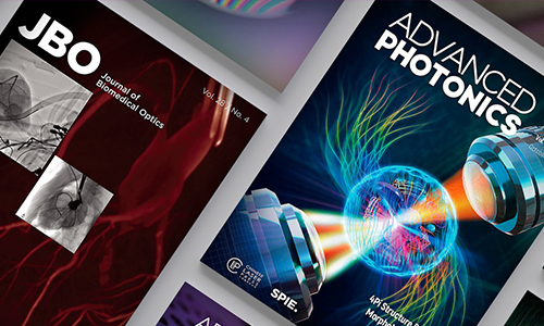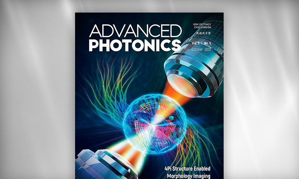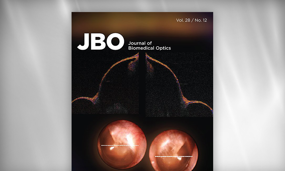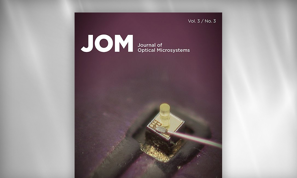
As a not-for-profit educational society, it is key to the SPIE mission to facilitate the sharing of knowledge and research within the scientific community. SPIE Publications, which includes the SPIE Digital Library, SPIE Press, conference proceedings, and 15 journals — produces, disseminates, and archives high-quality technical publications that meet the information needs of the optics and photonics community.
Part of your community
When publishing your research with SPIE, you are investing in your community.
We strive to deliver an author-focused experience with world-class service throughout the publication process. Publishing with SPIE ensures your research will find an engaged and receptive audience ready to learn from and cite your work.
Looking for technical content?
The SPIE Digital Library is the world’s largest collection of applied optics and photonics research with more than 650,000 pieces of scholarly content. Read the latest research published in SPIE Journals and Proceedings in the SPIE Digitial Library.
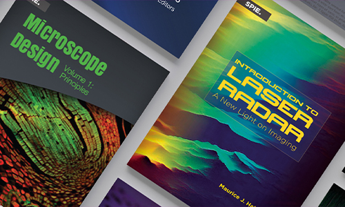
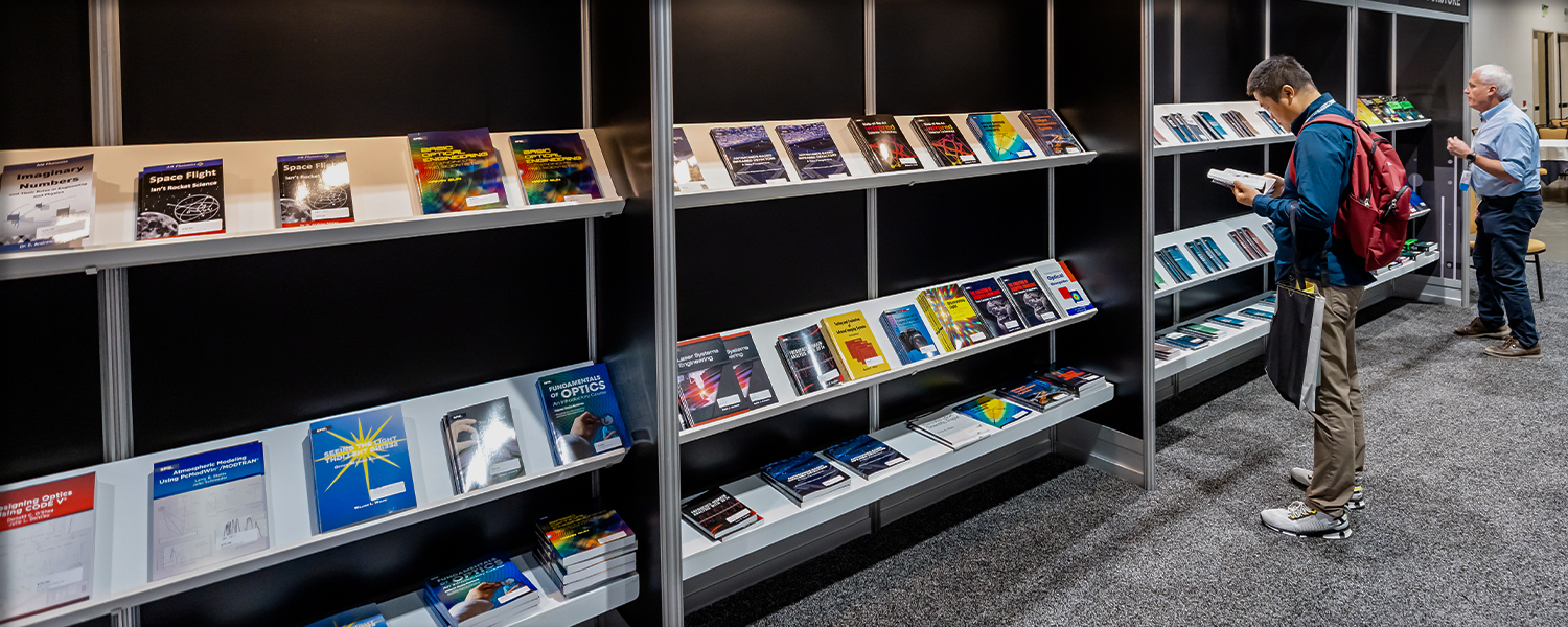
Browse the newest titles from SPIE Press in the SPIE Bookstore.
SPIE publications comprise the largest and most comprehensive collection of research papers and books on optics, photonics, and imaging applied science and technology. More than 650,000 publications are available in print and electronic formats to help you learn, stay current, solve technical problems, and bring your ideas to life.