An LED with 250% peak quantum efficiency
Although LEDs based on gallium nitride are widely available for lighting, they show disappointing high-power efficiency. In an ideal world, every injected electron results in the emission of a photon, giving 100% quantum efficiency. However, the transfer of electrical to optical energy is always accompanied by losses both of electrons and of photons. Accordingly, the total (external) quantum efficiency (EQE) is split up into the internal quantum efficiency (IQE) and the photon extraction efficiency (EXE). It is generally believed that electron (and hole) losses are the core reason for the efficiency reduction (droop) at high light power, reflected by a strong reduction in IQE for higher injected current.1
Several mechanisms have been proposed to explain the IQE droop. Among them are defect-related recombination or Auger recombination inside the light-emitting quantum wells (QWs) and electron leakage from them. Despite recent advances, clear quantitative experimental evidence for any of these mechanisms is still missing, and none of these proposals has received general acceptance. However, all these IQE droop models hold the rising carrier density inside the QWs responsible for the efficiency reduction. It therefore seems advantageous to lower the carrier density by using thicker QWs or by increasing their number. The former approach has already been successfully demonstrated experimentally,2 but the effect of adding more QWs is hindered by strong carrier accumulation in QWs located on the p-doped side of the LED.
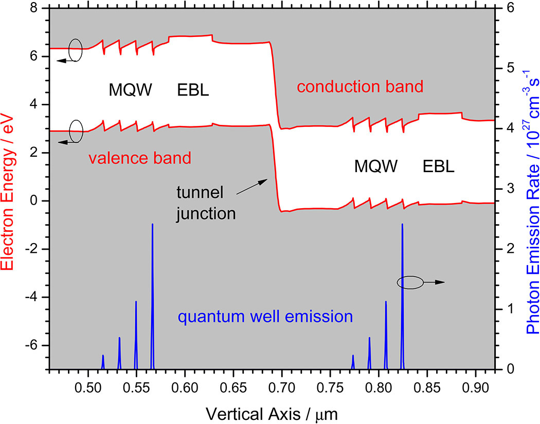
We have found a novel solution to this problem by inserting tunnel junctions into a multi-quantum-well (MQW) structure, without increasing either the thickness or number of QWs.3 Low-resistance GaN-based tunnel junctions have been demonstrated experimentally.4 Carrier recycling by the tunnel junction enables the repeated use of electrons and holes for photon generation inside the QWs. Figure 1 shows a two-stage LED with one tunnel junction separating two sets of four QWs. The photon generation in this device works as follows. Conduction-band electrons are injected from the left-hand side, recombine with valence-band holes within the first MQW stage, and then move inside the valence band to the tunnel junction, where they are transferred to the conduction band of the second MQW stage, so that they get a second chance to generate photons. Thus, the quantum efficiency could be as high as 200% if there were no losses. The emission profiles of both MQW stages are almost identical, but they still suffer from strongly non-uniform carrier distribution. Better performance is therefore expected with three tunnel junctions separating four QW pairs. Such a four-stage LED would enable up to 400% quantum efficiency.
We employed advanced numerical LED simulation to investigate these tunnel-junction design concepts based on experimental results for an eight-QW reference LED without tunnel junctions.5 The calculated performance characteristics show that the peak quantum efficiency at low power is 63% for the reference LED, 131% with one tunnel junction, and 253% with three tunnel junctions (see Figure 2). Even at high power, the four-stage LED exhibits a quantum efficiency well above 100%. It outperforms the alternative concept of merging all QWs into one thick active layer (a double-heterostructure LED).3 Note that the efficiency is plotted over the input power, instead of the input current, to account for the higher bias required to operate tunnel-junction LEDs. The photon extraction efficiency is constant in each case and remains close to the reference value of EXE=80%, even when considering tunnel-junction absorption. Ramping up the input power in any of these cases is accompanied by a higher carrier density in the QWs and causes a significant efficiency droop with increasing power. However, light output power (as shown in Figure 2) and wall-plug efficiency are strongly enhanced after tunnel-junction insertion, even at high power.

In summary, we propose a novel approach to LED efficiency improvement by inserting tunnel junctions into the MQW active region without changing the total thickness of active layers. This concept enables carrier recycling and high-power quantum efficiencies well above 100%. We are now working to further analyze and reduce the remaining efficiency droop.
Joachim Piprek provides on-demand simulation studies and consulting services in optoelectronics. He has been an invited guest editor for several journal issues on optoelectronic device simulation and has published three books, six book chapters, and more than 200 papers with close to 5000 citations.