Optics in space: One of the greatest adventures in human history
Vladan Blahnik joined ZEISS in 2001 as a lead system engineer and project leader for lithography optics, working on the development of projection lenses and illumination systems for lithographic scanners that would enable mass production of microchips. In 2008, Blahnik became the head of optical design at ZEISS' camera lenses division developing lenses for photography, cinematography, and digital-optical systems. Since 2018, he has held the role of senior optical systems engineer in ZEISS' Optical Design and Concepts department.
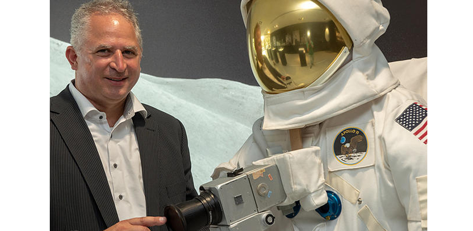
Blahnik was a plenary speaker at SPIE Remote Sensing 2021, where he discussed the camera lenses that ZEISS developed for NASA, as well as the the partnership between NASA, Hasselblad, and ZEISS.
What are some of your primary responsibilities at ZEISS?
I work in corporate research, and we are always on the lookout for technology and products, tracking trends and progress in technology and applications. We also consult with external partners in the industry, at research institutes and universities, and address these topics with innovation management and R&D groups in our various business units. ZEISS offers a wide range of products: medical technology, including ophthalmic devices and microsurgery systems; semiconductor manufacturing technologies, including lithographic projection systems and mask and wafer inspection optics; microscopy; metrology for quality inspection; and consumer products like camera lenses, binoculars, and eyeglasses.
I spent 17 years working in product development of semiconductor manufacturing and consumer products. For corporate research, we work on projects across all ZEISS business units, especially for products or methods that are new and still need to be established. My job as an optical systems engineer is to translate the application requirements into technical specifications and then find solutions with the relevant team. Other tasks include organizing ideas, and sharing and creating synergies between different ZEISS divisions. For example, there are similarities whether you're producing digital eyepieces for microscope applications, spotting scopes, camera viewfinders, or VR headsets.
What got you interested in working with lenses and space exploration?
Lenses first fascinated me while I was studying physics at the Technical University of Braunschweig; I pursued this interest in my doctoral thesis. At the university, we developed programs ranging from wavefront aberration calculations with ray tracing, to six-fold integrals for partially coherent wave-optical imaging. Thanks to ZEISS and LEICA, we had design data for various microscopes at our disposal. After trying to understand the theory behind these systems, my enthusiasm increased even more due to the strong connection between theory, experimentation, and practice, as well as the drive to keep improving the systems and bring them to market as viable products.
I came across the topic of "space exploration" purely by chance: In 2019, when we celebrated the 50th anniversary of the first Moon landing, the ZEISS communications department approached me: "Vladan, you know your way around camera lenses. Next week, 20 journalists from technical magazines will be visiting Oberkochen to write pieces on ZEISS' role in NASA's Moon landing. Could you give a lecture on the subject?" At the time I hardly knew anything about the subject, but, thanks to our historian Dr. Wolfgang Wimmer and my colleague Michael Rottler, I quickly amassed some excellent information. And I was able to add significant information to this thanks to our optical design archive at the Camera Lenses division.
That archive contains hundreds of files with data sheets, calculations, and notes taken by the optical designers for all photo and film lenses developed by ZEISS since 1946. We even have documents and data sheets from the early beginnings of camera-lens development at Carl Zeiss in Jena, around 1890. These documents, a fantastic resource, were transported along with 84 ZEISS employees and their families, who were brought from Jena to Oberkochen by the American military after WWII. I discovered detailed optics data, which included tolerance calculations for all the camera lenses used for the NASA space missions and their respective lab qualification reports, and I found valuable notes from legendary ZEISS optical designer Dr. Erhard Glatzel on various optical concepts for NASA requirements, and even a chronology of the development process of the lunar lens Biogon 5.6/60mm, with which almost all lunar-surface pictures were taken during Apollo missions 11 through 17. So, a lot of valuable material came to light that had lain dormant for 50 years.
For the Apollo mission, NASA decided on a camera fitted with a Reseau plate, which created a grid of cross-marks on the images. How did this help the astronauts take better images?
The camera lenses used on the Moon were what's known as photogrammetric. Object sizes and angular distances should be reconstructable from the images. The lens distortion was <0.008%, which is far better compared to a standard lens. You can see these small reference crosses created by the Reseau plate on every picture taken on the lunar surface. The astronauts took 360° panoramic images from several positions on the landing area. After the mission, those pictures were combined by NASA scientists and used to create a topographical map of the entire landing area.

Details of the Hasselblad data camera from 1969 and ZEISS Biogon 5.6/60 lens. Credit: ZEISS
What do you see as key elements in the future of photography in space exploration?
Recording and processing many images and data, i.e. computational imaging, have helped us capture fantastic images during space exploration with telescopes or cubesats. A recent example is the "recording" of the black hole in the center of the Messier 87 galaxy. The networking of many different data sources and the processing of this data, with the help of powerful image databases and machine learning methods, will be further expanded in the future. And we're already getting fantastic pictures from the Mars Perseverance Rover — the drone contains as many as 23 cameras! Some of the cameras help to control the drone, while others provide incredibly detailed moving images of the environment.
What do you consider the most critical recent developments in lens technology and optical design?
We all carry powerful imaging systems in our pockets: our smartphones. The miniaturization of both imaging and illuminating optical systems and photonic integrated circuits and their networking will be expanded even further in the coming years. 3D image acquisition sensors along with augmented reality applications will be further improved. Machine learning and other techniques will also be improved to better recognize or interpret objects along with seamless interaction between humans and digital objects.
Together with my colleague Oliver Schindelbeck, I recently published "Smartphone Imaging Technology and its Applications." Here we look at the market developments, technical requirements, optical design and technology of multi-camera systems, their image quality enhancements (like autofocus and image stabilization) and the implementation of various image representations through computational imaging such as portrait mode for bokeh or high dynamic range (HDR).
Without a doubt, digitalization was the key that unlocked a revolution in camera lens technology. Digital photography has created endless possibilities because the images are immediately available and transferable and can also be modified, combined, and processed.
Moving from the analogue to the digital age has also placed new requirements on the optical system and lenses. Aberrations such as lens distortion or vignetting can easily be corrected digitally. But removing aberrations digitally also has side-effects, such as in terms of contrast.
Nevertheless, the overall quality requirements of lenses have increased: Professional photographers zoom in on the finer details of an image in Photoshop, which in the analog past used to mean having to print out very large posters. This makes it easy to see imaging imperfections, like color fringes, due to chromatic aberrations or artefacts that result from camera image processing. In R&D today, you have to pay much more attention to the entire digital imaging chain when optimizing camera systems.
Which of your current projects are you most excited about?
I'm currently working on a number of different projects. We've developed various optical designs for LIDAR systems for autonomous driving, and the first ones are currently in the prototype phase. This is a prime example of the connection between optics and photonic integrated circuits and the co-optimization of both worlds.
I am also working on advancing EUV technology for optical lithography. In terms of the required measurement accuracy when qualifying the freeform surface mirrors in the projection system, we are talking about a few tens of picometers in surface deviations. That's incredible. It is important to systematically record all error contributions in the interferometric surface measurement process. For this purpose, we are expanding our simulation software and the methods of error assessment. This should benefit new EUV projection lenses with large numerical apertures, which we're working on now.
Related SPIE content:
A giant leap for humankind
| Enjoy this article? Get similar news in your inbox |
|


