Building the future with flexible electronics
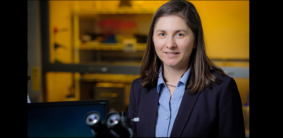
At SPIE Optics + Photonics 2022, Oana Jurchescu of Wake Forest University will offer answers to the question "can solution-processed organic thin-film transistors enable ubiquitous electronics?" Here she discusses her work with organic and hybrid electronic materials and devices.
What are some of your responsibilities as the Baker Professor of Physics at Wake Forest University?
At Wake we truly value the teacher-scholar ideal, with excellence being sought in research, teaching, and mentoring. Alongside teaching undergraduate and graduate physics classes and being one of the founding members of the Center for Functional Materials at Wake Forest University, I strive to build a research group that creates, innovates, and delivers solid scientific output that stands the test of time. I mentor undergraduate, graduate students, and postdoctoral researchers, and guide them in shaping long-term career plans. I am a strong advocate for diversity and inclusion in science, and I have established a strong tradition of mentoring women and underrepresented students. Such efforts benefit all group members since they have the opportunity to work in a team with a broad perspective and which represents more accurately the workforce they will join after leaving my lab.
You also head the Jurchescu group at Wake Forest. What is the focus of your work there?
The goal of my research program is to enhance the understanding of electronic processes in organic and hybrid electronic materials and devices, and to apply this knowledge towards improving their performance and expanding their functionality. The activities carried out in my lab range from fundamental to applied research and provide many opportunities for interdisciplinary student training. The projects expose students to state-of-the-art semiconductor processing and characterization techniques, training them to be the next generation leaders when they begin employment in modern environments focused on semiconductor technologies.
Would you briefly detail some of your lab’s research projects?
Fundamental studies on charge transport in organic materials and devices: This project focuses on (1) improving the fundamental understanding on charge transport in the bulk of organic semiconductors and at various interfaces, (2) providing accurate conclusions about the potential and limitations of organic semiconductors as opto-electronic materials, (3) designing and implementing device architectures that promote high performance.
Charge carrier transport in organometal halide perovskite devices: Hybrid organic-inorganic halide perovskite materials are strong contenders for many thin-film optoelectronic applications. But despite the remarkable demonstrations of high-performance solar cells and light-emitting diodes, all of which took place in a very short time, the nature and dynamics of the charge carriers remains unclear. In this project we study the structure and function relationships that define the interconversions between light, excitons, spins, and charge carriers in these materials, as well as the processes occurring at heterointerfaces involving them.
Molecular electronics: The growing demands for smaller and faster electronics have sparked the need for new componentry technologies. Molecular devices could address this challenge and complement the conventional silicon-based industry with smaller, cheaper, and more versatile applications. One of the simplest structures is represented by the molecular diode. This project aims at understanding charge transport mechanisms in molecular devices and developing efficient current rectifiers by exploiting structure-property relationships.
Large-area, low-cost flexible electronics: In this project, we develop methods for controlling thin-film order over a wide range of length scales to fabricate large area device arrays on flexible substrates. These devices are then tested for a variety of applications, such as tissue‐equivalent radiation dosimeters for cancer treatment, humidity, and chemical sensors, etc. In addition to the solution-based approaches used for thin-film manufacturing, we also explore solvent-free deposition methods such as laser printing. This low-cost, environmentally friendly, and high-throughput coating technique is compatible with flexible substrates and allows for simultaneous deposition, purification, and patterning of the semiconductor layer.

An example of a flexible device being researched by Wake Forest University. Credit: Ken Bennett, WFU
What led to your interest in the field of organic semiconductors?
Organic semiconductors (OSCs) are amazing materials for two main reasons. With an extraordinary chemical diversity, low-cost, and ease of processing, they are touted as impacting contemporary applications by providing an opportunity to incorporate electronics in non-traditional areas such as clothing, flexible, rollable applications, and bio-integrated applications. In doing so, they will contribute to significant societal benefits, ranging from the field of energy and environment to health and wellness, information and communication, entertainment, advertising, and more. At the same time, and equally important, organic semiconductors are intriguing materials with unique properties owing to the weak nature of their intermolecular interactions. Their physics is fascinating and quite often doesn’t follow any of the known theories from the solid-state physics textbooks. Trying to answer some of the fundamental scientific questions that these materials raise is provocative.
This year you won an National Science Foundation (NSF) Special Creativity Award to develop “OSCAR” — Organic Semiconductors by Computation on the Accelerated Refinement. What is the mission of OSCAR? What has been learned or developed through this project?
The project entitled “Organic Semiconductors by Computation on the Accelerated Refinement” — or OSCAR — is carried out under the auspices of the NSF’s Designing Materials to Revolutionize and Engineer our Future program, and it is performed in collaboration with Professors John Anthony (synthesis) and Chad Risko (computation/modeling) at University of Kentucky, and Professor Lynn Loo (processing and structural studies) at Princeton University. The solid-state order is the key determining factor for a broad spectrum of optical and electronic properties of organic semiconductors but predicting it is still out of reach. This project aims to accelerate the development of optimized materials by deploying models for predicting the molecular structure required to achieve on demand solid-state arrangements. Working collaboratively, we developed a tight feedback loop among molecular design and synthesis, materials processing and characterization, device testing and optimization, multiscale theory and computation, and large-scale data curation and machine learning. OSCAR has enabled the development and deployment of in silico OSC design paradigms to shorten the path from concept to commercialization by bypassing the lengthy optimization process and providing guidance to rapidly select and synthesize high-performance molecular building blocks and materials. Our efforts resulted in the discovery of new classes of high-mobility OSCs, the development of processing protocols to produce large-area, stable devices, and a pathway to break into real applications in the field of radiation sensors.
What do you see as the future of organic semiconductors? What would you like to see?
Organic light emitting diodes (OLEDs) have become a mature technology and OLEDs are now present in most mobile phone displays, but also other displays. I hope that other organic devices (solar cells, transistors) will soon become omnipresent in our lives to offer new applications that are not possible to achieve with conventional semiconductors, secure our well-being, and shape major fields. Collectively, these new components could fundamentally change the way we interact with electronics and unlock new paradigms for addressing major challenges (and possible crises) laying ahead of us regarding sustainability (transportation, food, energy), healthcare, and environment.
What topics will you be covering in your plenary talk, “Can solution-processed organic thin-film transistors enable ubiquitous electronics?”
In this talk, I will first provide a historical perspective of the development of organic thin-film transistors (OTFTs) and then discuss the factors that impact the performance of these devices. I will emphasize the difference between the material and device properties and how non-idealities in operation can lead to errors in extracting quantitative information about these properties. I will address some of the key metrics typically referred to in benchmarking the efficiency of OTFTs and discuss the interplay between these parameters and the requirements for transitioning from a lab setting into consumer applications. I will also discuss possible alternative applications for OTFTs that have sub-par performance in an attempt to broaden their applicability.
| Enjoy this article? Get similar news in your inbox |
|


