40 years on, SPIE brings lithography community to Silicon Valley again for premier event for industry

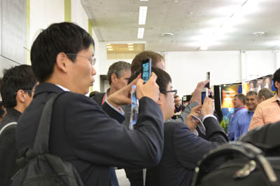
The "wow factor" is in evidence throughout events at SPIE Advanced Lithography; above exhibition visitors capture a demonstration at an exhibitor's booth in last year's show.
BELLINGHAM, Washington, USA -- Extreme ultraviolet lithography (EUV), 3D integration, and the Internet of Things will be among critical technologies featured at SPIE Advanced Lithography 2015 22 to 26 February in San Jose, California.
The SPIE symposium is the year's premier lithography event, bringing together leading industry professionals and academic researchers for conference presentations, panel discussions, a suite of professional development courses, an exhibition featuring major industry suppliers, and numerous networking opportunities.
SPIE 2015 marks the 40th anniversary of the event, organized by SPIE, the international society for optics and photonics.
Conference topics are extreme ultraviolet lithography; alternative lithography; metrology, inspection, and process control; patterning materials and processes; optical lithography, DPI manufacturability, and advanced etch technology for nanopatterning. Panel discussions will explore metrology for 3D devices and dimensional scaling.
SPIE 2015 will once again provide the unique and primary forum for meeting and interacting with a wide range of industry experts, researchers, and other key players in the field, noted symposium chair Mircea Dusa of ASML US, Inc., and symposium cochair Bruce Smith of the Rochester Institute of Technology. The event is unmatched as a forum for facilitating collaboration and networking, and for sharing the latest developments in areas of central importance in lithography, they said.
Plenary presentations from Xiaowei Shen, director of IBM Research in China; Tsu-Jae King Liu of the University of California, Berkley; and Alan Willner from the University of Southern California will open the conference program on Monday 23 February.
Shen will outline the technical challenges of building Internet-of-Things (IoT) cloud platforms and describe his experience in creating IoT solutions in fields such as renewable-energy forecasting and chronic-disease management.
Liu will detail challenges in transistor scaling and the cost-effective 3D integration required to sustain the growth of the semiconductor industry.
Willner will give an overview of the National Photonics Initiative (NPI) and detail recent success in advocacy for the semiconductor industry -- including the announcement in November of a $110 million matching funding commitment from the U.S. Department of Defense for a new Integrated Photonics Institute for Manufacturing Innovation.
Exhibiting companies including ASML, Zeiss, Mentor Graphics, ShinEtsu, TOK, Synopsys, JSR Micro, Tokyo Electron, Physik Instrumente, and Brewer Science will show the latest developments in equipment, software, and techniques, in the two-day exhibiton, 24-25 February.
New Fellows of SPIE from the lithography community will be recognized and the Frits Zernike Award for Microlithography will be presented.
The largest lithography expert gathering on the globe, SPIE 2015 is expected to host more than 2,400 individuals from more than 30 countries.
SPIE is the international society for optics and photonics, a not-for-profit organization founded in 1955 to advance light-based technologies. The Society serves nearly 235,000 constituents from approximately 155 countries, offering conferences, continuing education, books, journals, and a digital library in support of interdisciplinary information exchange, professional networking, and patent precedent. SPIE provided $3.4 million in support of education and outreach programs in 2014.
Contact:
Amy Nelson
Public Relations Manager
amy@spie.org
+1 360 685 5478
@SPIEtweets