High performance, stable solution-processed thin-film transistors
Most current active matrix LCDs use amorphous silicon (a-Si) thin-film transistors (TFTs) as pixel switching devices. A great disadvantage of a-Si is the limited mobility of 1cm2/Vs (volt second), which is insufficient for advanced display technologies such as 8K ultra high-definition, large-size TVs, and organic light emitting diode (OLED) displays. One promising alternative is low-temperature polysilicon, which exhibits mobility values of 100cm2/Vs. However, it is not suitable for large area fabrication because of its non-uniform crystal growth, which is why upscaling is limited.1
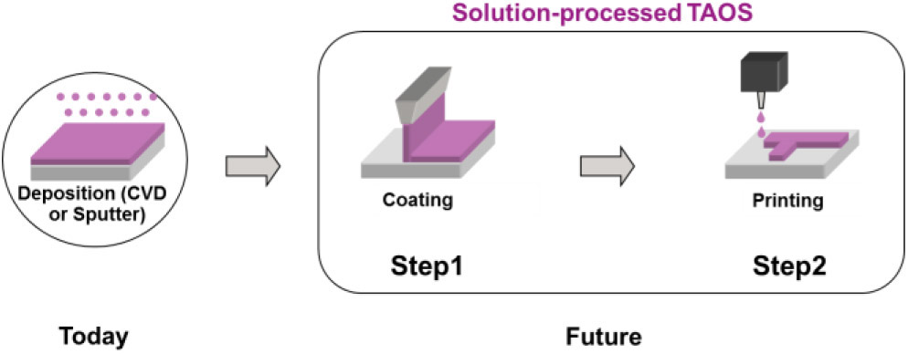
Solution processed metal-oxide semiconductors are good candidates to replace a-Si-based TFTs as switching devices for display applications and for large area deposition because of their high mobility, transparency, uniformity, and low manufacturing costs.2,3 There are two specific advantages of solution-based materials, the possibility to combine different precursor systems and the direct printing of transparent amorphous oxide semiconductor (TAOS) structures (see Figure 1). However, the reliability of such metal-oxide based semiconductors is not yet satisfactory.

We are working on solution processable materials for TFTs, such as semiconductor, passivation, and dielectric, which allow an increase in performance compared to a-Si, a significant lowering of process costs, and large area deposition compared to sputtering.4This is achieved by using metal-oxide-based materials5,6 that are deposited from solution and processed fully under ambient conditions.

We prepared a stable TFT under atmospheric conditions with iXsenic S, a solution-processable product from Evonik Industries. We used iXsenic P, a solution-based hybrid polymer, as the passivation layer. Both materials were deposited by slot die coating or spin coating. The iXsenic S is a solvent-based, organo-metallic precursor system that is formulated into inks. These materials are optimized for homogenous coating properties, long shelf-lifetime, and a robust process. The iXsenic P prevents oxygen and moisture adsorption on the semiconductor surface, and it can be directly patterned by a simple UV lithography step with the i-line (λ = 365nm) of a low-pressure mercury lamp.
We fabricated a bottom gate, bottom contact (co-planar) TFT by spin coating iXsenic S on highly doped silicon substrates substrates with pre-structured source and drain contacts. After annealing the film at a maximum temperature of 350°C, we patterned the layer by using a wet etch process to suppress the gate leakage current. The passivation of the semiconductor was done by spin coating the iXsenic P. The film was patterned by UV lithography and then transformed into a dense film on a hot plate at 250°C.
The electrical characteristics were measured with a semiconductor parameter analyzer under ambient conditions. Figure 2 shows a typical transfer curve of iXsenic S in the co-planar device. The device's turn-on voltage is normally 0V to -3V, with an off-current below 5fA/μm (drain current per channel width, IDaaaW) for a patterned semiconductor. In this simple TFT layout, an electron mobility of 12cm2/Vs is achievable using the linear model. It is sufficient to drive OLEDs.
Besides the initial performance (mobility, on-off ratio, and onset voltage VON), the TFT's electrical stability under realistic conditions is important for display applications. To investigate the stability of iXsenic S, we stressed devices passivated with iXsenic P with constant negative and positive gate bias. The stress tests were done under ambient atmosphere and elevated temperature T of 60°C. Figure 3 shows the initial transfer curves as well as the negative and positive gate bias stress of a device with a patterned iXsenic S layer and a non-patterned passivation film. The applied gate bias was -20V for the negative bias temperature stress and 20V for the positive bias temperature stress, respectively. Additionally, we applied a voltage of 5V between the source and drain contacts. The onset voltage-shift for both stress measurements was less than 0.5V after 2000 seconds. Adsorbed moisture and oxygen at the semiconductor surface were assumed to be responsible for the bias stress instability.7 These results show that iXsenic P is an excellent passivation layer to avoid adsorption from ambient air. The relatively high off-current is not caused by the semiconductor or the passivation, but by the noise threshold of the automated measurement system (∼1nA) used for stress tests.

In addition to a high performance semiconductor solution processed at a temperature of 350°C, where mobility values above 10cm2/Vs are achievable, we are working on systems that allow access to substrates such as polyethylene naphthalate (PEN) or polyethylene terephthalate (PET), whose cost is more attractive. Figure 4 shows a transfer curve of iXsenic that is tuned for a process at a maximum temperature of 160°C. The curing was done for 2h. Currently, this material achieves a mobility of 2cm2/Vs with an onset voltage close to 0V.

In summary, we have presented a semiconductor that exhibits high electron mobility, low off-current, and good electrical stability when passivated with iXsenic P. Furthermore, these solutions are suitable for large area deposition, such as slot-die coating or ink-jet printing, because of their ability to form smooth and homogeneous layers. We also have developed a semiconductor that is compatible with processing on PEN or PET foils. Wet chemical processing opens the possibility of direct printing of electronic devices, which offers a cost advantage compared to sputtering processes. The next step will be upscaling to larger substrate sizes and the integration into a production line.
Felix Jaehnike received his diploma in electrical engineering from the Ruhr-University Bochum in 2011. He is working as a PhD student at Evonik. His research involves the stability of metal-oxide semiconductor thin-film transistors.
