Triple patterning in 10nm node metal lithography
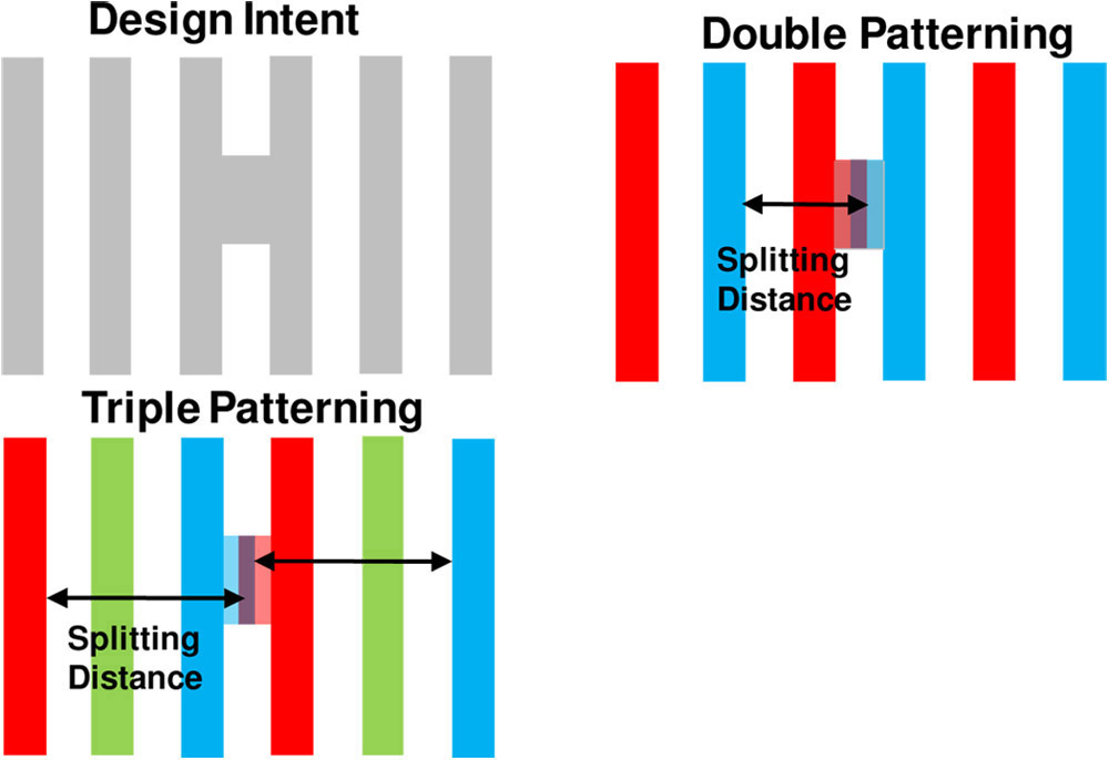
The local metallization layers of logic products are historically the densest layouts to lithographically pattern and are key drivers of product density (and therefore cost). Due to delays in extreme-UV (EUV) lithography and difficulties in applying other resolution-enhancement technologies (RETs)—such as double-patterning methods—triple-patterning technology (TPT) is a strong option for handling the local metal layers of the upcoming 10nm logic technology node (∼ 44–48nm minimum feature pitch). Several TPT methods, including ones developed by us, are being considered in different product areas of semiconductor manufacturing.1, 2 For advanced logic metal layers, the main TPT option assumes a process flow known as litho-etch-litho-etch-litho-etch (LELELE). In this flow, the final substrate pattern is the logical OR of three successive lithography+etch sequences, each sequence using a single traditional lithography exposure and a single etch step (see Figure 1).
The use of LELELE TPT in a product design and production flow involves the following steps: design of TPT-compliant layout; design verification; decomposition of the layout into the three TPT single-exposure wafer targets (via TPT decomposition software); RET/optical proximity correction (OPC) steps for each single-exposure wafer target; OPC verification; mask data preparation; mask manufacture; and wafer processing in the fabrication facility (fab). There are many difficulties in achieving a high-yielding, cost-effective TPT process. Here, we first look at problems in mask manufacture and wafer production flow, especially cost, turn-around time, and the logistical challenges of tripling the number of mask and fab process steps per layer. However, the complexity and process control requirements of a TPT mask and wafer flow also increase substantially. Moreover, potential negative interactions can cause device failure between feature edge placements from the different litho-etch steps.3 Consequently, individual feature critical dimension (CD) and overall control tolerances in a TPT process must be significantly tighter than in a single-exposure process for the same device layer.
Design and mask synthesis (i.e., decomposition, RET, OPC, and OPC verification) pose different but related difficulties. Designers must be able to confidently create and verify TPT-compliant layouts. This requires accurate and sufficiently flexible design rules. Figure 2 shows examples of basic TPT design rules for the metal1 layer of standard cells. The design flow must also be able to quickly and accurately verify the physical and electrical integrity of the full-chip final design target. Mask synthesis cost and turn-around time are definitely affected by the tripling of the number of processing steps. However, a bigger risk would be if the increased accuracy requirements could not be met. Fortunately, the RET, OPC, and OPC verification methods developed for DPT can be extended to successfully handle TPT requirements in these areas.

An even more fundamental TPT mask synthesis challenge exists in the layout decomposition step. Production-worthy TPT decomposition methods are not yet fully defined and validated. Currently, the two most plausible approaches are extension of existing DPT decomposition methods (see Figure 3), and development of full TPT decomposition algorithms. The advantage of the first approach is that DPT methods are well known, trusted, available, and fast enough to run on full-chip layouts. A main drawback is that it is less likely to result in a decomposition solution for layouts that are TPT compliant. This can lead to a TPT-compliant design being decomposed in an unmanufacturable manner. Another drawback of extending existing DPT methods is difficulty in achieving similar feature density for all three masks. Mask density imbalance can lead to degraded overlay and CD control.

We have proposed several TPT decomposition algorithms.2 The quality of results can vary strongly, as better algorithms can enlarge the set of layouts that are TPT-compliant, leading to solutions that have a smaller layout area and are more manufacturable (see Figure 4).4 The main drawback of full TPT algorithms is that their turn-around time/memory performance is not yet sufficient for full-chip decomposition (see Figure 5).5 With these performance limitations, the industry must do TPT decomposition individually on smaller cells and layout blocks, then use correct-by-construction design rule and design practice approaches to ensure the entire chip becomes TPT compliant. Fortunately, TPT full-chip compliance can be easily and quickly verified using extensions of existing DPT software (e.g., design rule constraints or OPC verification).


In summary, TPT patterning is a serious option for local metal layers in next-node logic processes. Several design and process techniques developed for DPT can be reused in TPT. However, significant challenges remain. The biggest process challenges are cost and control. The biggest design and mask synthesis challenges are the development and coordinated deployment of TPT decomposition algorithms. Our current work focuses on improving TPT algorithm applicability to larger layout sizes for 10nm node design rule and process integration development.
Sincere thanks for helpful discussions to Vincent Wiaux and Peter De Bisschop from IMEC.
Kevin Lucas joined Motorola Semiconductor in 1994 after completing his PhD in electrical and computer engineering at Carnegie Mellon University. In 2006 he joined Synopsys, where he currently is the RET and OPC product engineering manager.
University of Texas at Austin