Electrically driven photonic crystal cavities yield low-power optoelectronic devices
Optical interconnects in next-generation computing promise major performance enhancements and vast reductions in system power consumption. Present embodiments of optical information transmission range from traditional long-haul fiber-optics to intra-data center communication. To scale further—to intra-board or on-chip optical interconnects—appropriate semiconductor sources must be developed. And to be competitive with pre-existing electrical interconnects, optical links should aim for a total energy target of 10 femto-Joules per bit (fJ/bit).1
To attain the proper targets for low power consumption and speed, photonic crystal cavity devices have been explored as potential solutions.2 By possessing a wavelength-size cavity, the amount of dielectric material that must be controlled for a desired function is reduced, as is the corresponding energy. Until now, the ability to electrically harness the superior capabilities of photonic crystal cavities has remained elusive because of complicated fabrication procedures.3 We have developed a new platform to form a lateral p-i-n junction in gallium arsenide (GaAs) that efficiently controls cavities and enables ultra-low power operation of lasers, LEDs, and modulators.
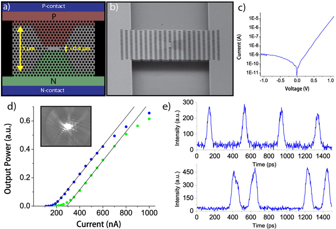
Our approach to solving the problem of electrical injection into 2D polycarbonate membranes is to use a lateral junction formed by ion implantation: see Figure 1(a).4 This contrasts with previous vertical junction approaches as the current pathway can be lithographically defined with high precision. We used a series of aligned electron-beam lithography steps along with optimized ion implantation and thermal annealing recipes to create devices: see Figure 1(b). A typical room temperature current-voltage plot—see Figure 1(c)—shows excellent rectifying diode behavior. Current densities above 10kA/cm−2 are estimated and simulations show that the injected carriers are concentrated at the cavity center.
At cryogenic temperatures we observe continuous wave lasing from internal quantum dot emitters when we drive our electrically contacted photonic crystal cavities.5 Figure 1(d) shows lasing pump power data for 50K and 150K along with fits that give 181nA and 287nA as threshold currents, respectively. These values are the lowest reported for any electrically pumped laser and represent an improvement of three orders of magnitude over previously demonstrated electrically driven photonic crystal lasers. At room temperature we find that our devices no longer laser, as the cavity loss is too excessive for the given quantum dot gain.
Room temperature LED operation presents interesting new physics that can be exploited for ultrafast modulation.6 We observe that our rapid thermal anneal step modifies the confinement properties of our quantum dots, and in doing so allows carriers to be ejected extremely fast. Figure 1(e) shows the direct electrical modulation of our LEDs at room temperature, giving a speed of 10GHz for a non-return-to-zero pattern. The energy consumed during these operations is only 0.25fJ/bit, which is the lowest control energy for any optical transmitter. Since our cavity emits in only a few spectral modes, the LED is essentially single-mode and therefore useful for sending information, just like a traditional laser.

The lateral p-i-n junction can be applied to several other designs not limited to sources in 2D membranes. Figure 2(a) shows a fabricated 1D nanobeam and its corresponding output optical spectrum and IR emission pattern.7 Interestingly, the electrical and optical properties of our nanobeam LEDs are remarkably similar to our 2D structures, despite their tiny conducting cross sections, indicating that these devices could also be employed as efficient sources. Finally, in Figure 2(b) we show a very different application of our lateral junction now used as a fiber taper-coupled external modulator.8 Here, the diode injects charge into the cavity region, which can tune the transmission resonance of light flowing through a fiber taper with control energies <1fJ/bit.
In summary, the rapidly growing field of optical interconnects is poised to revolutionize the paradigm of information transmission at the computer scale. Radically designed approaches, such as active and electrically driven photonic crystal cavities, are crucial for future device components to operate at sufficiently low power. Going forward, we will explore methods to attain room temperature lasing and higher output power efficiencies with different material systems. The progress in this work will be an important step for the design of practical and integrated photonic crystal cavity devices for diverse applications in the future.
Gary Shambat holds a BS in electrical engineering from the University of Virginia in Charlottesville, VA, and an MS in electrical engineering from Stanford University. He is currently working toward a PhD in electrical engineering with Jelena Vuckovic.
Bryan Ellis received his BS in electrical engineering from Princeton University and MS in electrical engineering from Stanford University. He is currently working toward a PhD in electrical engineering.
Jan Petykiewicz holds a BS in electrical engineering from the California Institute of Technology (Caltech) in Pasadena, CA, and is currently working toward MS and PhD degrees with the nanoscale and quantum photonics group in the department of electrical engineering.
Jelena Vuckovic, who has a PhD from Caltech, has been a faculty member in Stanford University's electrical engineering department since 2003, and is currently an associate professor. Her research focus is experimental nanophotonics and quantum photonics.