193nm immersion lithography: Status and challenges

This article is a comprehensive review of 193nm immersion lithography. It will be focused on the materials and processes rather than the optical system of the tool. Some of the results are from the author's previous publications. This is the first of five parts; each part is relatively self-complete.
History and status
193nm immersion lithography (193i) has been accepted by IC manufacturers as a manufacturing patterning solution at least down to the 45nm half-pitch node. Immersion lithography is a lithography enhancement technique that replaces the usual air gap between the final lens element and the photoresist surface with a liquid medium with a refractive index greater than one. The smaller wavelength in the liquid allows the imaging of smaller features and water is currently used as the liquid. Fig.1(a) shows a sketched diagram of the final lens and wafer.
The immersion technique was first introduced by Carl Zeiss in the 1880s to increase the resolving power of the optical microscope. Introduction of the immersion technique into modern lithography was suggested in the 1980s. It attracted the IC industry's attention in 2002 when 157nm lithography was delayed by several technical problems. Since then the development of 193i has been incredibly fast. In the immersion workshop organized by Sematech in July 2003, scanner suppliers showed their development plans of the 193i scanners. Sematech and its member companies re-oriented their development resources from 157nm to 193i. In August 2004, the first 193i full-field scanner (ASML AT1150i, 0.75NA, α-tool) was delivered to Albany Nanotech and used for the early immersion process learning. According to a sales report, through December 2006 more than 30 193i scanners have been sold to IC manufacturers worldwide.
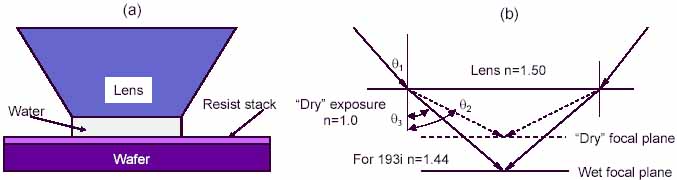
Figure 1. (a) A sketched diagram of 193i exposure head. Water fills the gap between the final lens and the wafer. The water injection and confinement system is not included in the diagram. (b) Optical paths of two-beam interference for both "dry" and 193i exposures. (Click to enlarge.)
The introduction of water into the gap between the final lens and wafer changes the optical paths of exposure light. Fig.1(b) shows two-beam interference exposures in "dry" and "wet" situations for comparison. The exposure beams pass through the air or water gap and are focused on the wafer surfaces. Refractions occur at the interface of lens/air for the "dry" exposure or lens/water for the immersion exposure, as sketched in Fig.1 (b). According to the Snell's law, the following relation dictates the refraction angles,
![]()
where q1 is the incident angle at the interface; q2 and q3 are the refractive angles corresponding to "dry" and immersion respectively. It is obvious from Eq.(1) that the introduction of water alone does not change the NA. However, the water does reduce the refractive angle, i.e., q2 > q3, increasing the depth-of-focus (DOF) of exposure. In the high-NA situation, the paraxial approximation can not be applied; and the Rayleigh DOF has to be modified to include the contribution of high incident angle beams 1, 2.
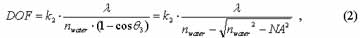
where k2 is the process factor. The contributions of the illumination settings, mask, and process to the DOF can be included into the factor k2.
Exposing a pattern with a pitch p, the incident angles can be calculated by sinq2 = λ/p for the "dry" exposure and nwater×sinq3= λ/p for the immersion exposure. The DOF improvement of immersion vs. "dry" can be obtained as
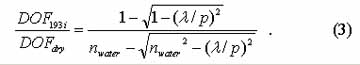
The improvement in DOF is at least the refractive index of the fluid, and gets larger for the smaller pitches.2 For example, 90nm dense lines were printed by a "dry" and an immersion tool with the same mask and illumination settings (0.75NA). About 2× DOF was obtained with the immersion exposure.3
Another advantage of the immersion technique is that it enables the lens designs with numerical apertures greater than 1.0 - hyper-NA 193nm immersion lithography. The NA of a "dry" exposure system does not go beyond 1.0; otherwise, the exposure light will be totally reflected back at the lens/air interface -- totally internal reflection. With water immersion, the maximum NA approaching nwater=1.44 is possible. Currently, 193i full-field exposure systems with 1.2NA are available in the market; and 1.35NA capability is under design. It appears that the hyper-NA 193i will provide lithography solutions down to 45nm half-pitch.
Apart from the gains -- DOF enhancement and hyper-NA lens design, 193i brings various process challenges. The first challenge is leaching, where the photo-acid generator (PAG), quencher, and other small molecular components in the resist can leach into the water. This leaching not only degrades the resist performance but also contaminates the water. The contaminated water can further contaminate the lens and wafer stage of the scanner. Water can also permeate into resist film, causing resist swelling and changing its photochemical properties. Prior to the availability of low-leaching resists, topcoat is an effective solution to block both the leaching and the water uptake.
Topcoat is spin-coated on resist and is transparent at 193nm wavelength. It serves as a barrier layer, enabling the regular 193nm resists -- "dry" resists -- to be used in the wet process. The topcoat layer is removed after exposure / post exposure bake (PEB) and before pattern development. According to their solubility in regular aqueous TMAH developer, there are two types of topcoats - developer-insoluble topcoat and developer-soluble topcoat. Developer-insoluble topcoat can only be removed with a specific topcoat solvent -- an additional step as well as a process-tracking module is needed for removing the topcoat, as sketched in Fig. 2(a). Therefore, developer-insoluble topcoat is not production favorable, and it was quickly followed by developer-soluble topcoats. Developer-soluble topcoat can be dissolved by regular aqueous TMAH developer. Therefore, the topcoat removal step can be done in the develop module and integrated into the development step, as sketched in Fig. 2(b). However, compatibility of the resist and topcoat has to be considered; and the process parameters have to be aligned to obtain the best lithography process window.
Resist processes without top protection coatings are the preferred solution for introduction of 193i lithography into mass production. These simplified processes, as sketched in Fig.2(c) do not need separate coating and baking steps for the topcoat material and thereby reduce cost of ownership and offer fewer sources for defects. Conventional 193nm resists that are optimized to optimum performance upon "dry" exposures are not suitable for being used in immersion lithography without topcoats, because resist components show (before and/or after exposure) at least some solubility in water and leaching into water, thereby deteriorating lithographic performance. Without a topcoat as a barrier layer, the selection of components for single-layer 193i resists that can be used without top coatings is challenging, since minimized leaching and superior lithographic performance are to be met simultaneously. Material innovation is the key for non-topcoat processes to supercede topcoat processes.

Figure 2. Process flow comparison of resist stack with solvent-soluble topcoat (a), developer-soluble topcoat (b), and without topcoat (c). (Click to enlarge.)
Immersion-related defects are another challenge to the 193i process. The water between the front lens and wafer forms a meniscus that moves with the exposure head across the wafer. Various physical and chemical interactions between the water and resist stack occur, leading to water immersion-related defects: Bubbles in the water can distort the exposure image, water droplets left on the wafer surface may deteriorate the local resist performance, and water can transport particles to the wafer surface and deposit them there. With an un-optimized 193i process, typically 4-20% more defects may be added to a wafer than that of "dry" 193nm lithography. The limitations on the process yield caused by immersion defects must be solved before bringing 193i lithography into high-volume production.
With hyper-NA 193i exposure, the maximum incident angle of the exposure light on the resist stack is high. For example, corresponding to 1.3NA, the maximum incident angle is sin-1(1.3/1.44) = 64.50; while at 0.75NA of 193i, the maximum incident angle is only about 31.40. The high incident angle will cause the contrast loss of the transverse magnetic (TM) imaging component. Fig.3 shows a diagram of the two-beam interference. Electric field of the incident beams ![]() can be divided into two components: one in the incident plane (
can be divided into two components: one in the incident plane (![]() ); and another perpendicular to the incident plane (
); and another perpendicular to the incident plane (![]() ), where TM and TE denote transverse magnetic and transverse electric fields, respectively.
), where TM and TE denote transverse magnetic and transverse electric fields, respectively. ![]() and
and ![]() . After the light is focused on the wafer surface, its total intensity is
. After the light is focused on the wafer surface, its total intensity is
![]()
The TE components (![]() and
and ![]() ) are parallel to each other, and their superposition has no relation to the incident angle. However, the TM components (
) are parallel to each other, and their superposition has no relation to the incident angle. However, the TM components (![]() and
and ![]() ) form an angle of 180°-2q3; and the superposition depends on the incident angle by a factor of cos(2q3). At hyper-NA exposure, the cos(2q3) is much smaller than one and destroys the TM contrast. Therefore, illumination with only the TE component -- i.e., TE polarized illumination - has been suggested for hyper-NA exposure. The high incident angle will also lead to a high reflection at the interfaces of the resist stack and make the reflectivity control very difficult. Especially when patterns with different pitches are exposed, the incident angles of the exposure lights are scattered in a broad range. Reduction of reflections from different incident angles is extremely challenging for a single-layer BARC. Different BARC strategies have been proposed for hyper-NA imaging, for example the thick organic BARC approach and double-layer BARC approach 4.
) form an angle of 180°-2q3; and the superposition depends on the incident angle by a factor of cos(2q3). At hyper-NA exposure, the cos(2q3) is much smaller than one and destroys the TM contrast. Therefore, illumination with only the TE component -- i.e., TE polarized illumination - has been suggested for hyper-NA exposure. The high incident angle will also lead to a high reflection at the interfaces of the resist stack and make the reflectivity control very difficult. Especially when patterns with different pitches are exposed, the incident angles of the exposure lights are scattered in a broad range. Reduction of reflections from different incident angles is extremely challenging for a single-layer BARC. Different BARC strategies have been proposed for hyper-NA imaging, for example the thick organic BARC approach and double-layer BARC approach 4.

Figure 3. Two-beam interference. The electric field of the incident beams can be divided into two components -- TE and TM. The TM components cannot form enough contrast at hyper-NA.
Fig.4 shows a stack of lens/immersion fluid/resist/BARC system, which mimics the immersion exposure head. According to Snell's law, ![]() . As labeled in Fig.4, q1,3,4 are the incident angles of the exposure beam at the interfaces of lens and fluid, fluid and resist, and resist and BARC (topcoat is not included in the discussion) respectively. Apparently, the maximum effective NA is equal to min[nlens, nfluid, nresist], i.e., the further increase of NA is limited by the refractive index of lens, fluid, and resist. Therefore, high refractive index materials are the key to the further increase of NA.
. As labeled in Fig.4, q1,3,4 are the incident angles of the exposure beam at the interfaces of lens and fluid, fluid and resist, and resist and BARC (topcoat is not included in the discussion) respectively. Apparently, the maximum effective NA is equal to min[nlens, nfluid, nresist], i.e., the further increase of NA is limited by the refractive index of lens, fluid, and resist. Therefore, high refractive index materials are the key to the further increase of NA.

Figure 4. Optical path of the exposure beam in a lens/immersion fluid/resist/BARC system
Encouraged by the great success of the water immersion, various high-refractive-index (RI) materials, including high-RI immersion fluids, high-RI lens materials, and high-RI resists, are being developed. A high-RI fluid of n=1.65 is now available and ready to be tested by scanner suppliers.5 Various high-RI lens materials have been screened. Initial results have demonstrated that LuAG has a RI of ~2.2 and can be a strong candidate for making a high-RI lens6. Introduction of sulfur into photoresist polymers can significantly increase their refractive index.7 Second-generation 193i with an immersion fluid of n=1.65 and lens of n=2.0 is expected to achieve a NA of 1.55 and third-generation 193i will eventually push the NA to 1.65. Based on this projected progress, 193i+ is becoming a strong competitor to EUV lithography for the 32nm half-pitch node.8
Yayi Wei is a staff engineer of Qimonda North America Corp (formerly the Memory Product Division of Infineon Technologies North America Corp.) and a member of SPIE working on advanced lithographic process development and photoresist evaluation.


