Microfabricating 3D structures by laser origami
Digital microfabrication techniques such as laser direct-write (LDW) offer a viable alternative for generating 3D self-folding designs. These designs enable novel electronic and optical functionality within limited form factors not possible via current 2D structures. The approach requires self-folding at the microscale where manual or mechanized actuation of the smaller structures is not practical. LDW techniques allow micromachining and printing of 2D patterns and/or structures, deposition of an actuating layer, and controlled activation of each actuation layer to trigger the folding of single or arrayed microassemblies. As a result, the ability to induce folding (either sequentially or in parallel) on nontraditional types of substrates (i.e., polymers and composites) for developing complex and novel arrays of 3D microstructures is now possible.
The ancient Japanese art of paper folding known as origami allows the transformation of flat patterns into 3D shapes. A similar approach can be used to generate 3D structures comprising electronic, optical, or mechanical devices that cannot be fabricated using conventional layer-by-layer—i.e., planar—lithographic methods. Typically, 2D patterns or structures are first generated with lithography, followed by some alternative technique for bringing these structures out of the plane. For example, folded features from lithographically defined flat regions and their corresponding hinges have been produced after activation by stresses originating from bimetallic films, as shown by Stellman and co-workers,1 or from ion implantation, as shown by Arora and colleagues.2
While photolithography is advantageous from a yield aspect, it suffers from a lack of flexibility, which translates to limitations on the realizable geometries. The overarching challenge is to move away from traditional planar semiconductor photolithographic techniques, which severely limit the type of materials that can be integrated and the kinds of substrates that can be used. The laser origami technique allows for the design and fabrication of arrays of 3D microstructures, where each element is preprogrammed with the information required for building itself. In other words, each microstructure can be actuated independently of the rest. This represents a complete paradigm shift from current approaches because it enables full control of the folding of each element within the array, rather than relying on batch processing. Application of these folded microassemblies would make possible the development of highly complex and interconnected electrical, optical, and mechanical 3D systems.

At the Naval Research Laboratory, we have demonstrated several implementations of laser origami for generating 3D meso- and microstructures on various types of substrates. Laser origami applies LDW techniques to generate the structural elements and functional patterns required for self-folding in three simple steps (see Figure 1). First, we generate the features through laser microfabrication, then selectively place the active elements by laser transfer or laser cutting, and, finally, we use laser curing, heating, or ablation to achieve out-of-plane actuation. Use of a single tool (the laser) represents a significant streamlining of the overall process.
In one of our implementations, the folding of copper films with thickness ranging from 0.1 to 1μm was demonstrated over bending angles from 0° to 180° as a function of laser intensity. This was achieved by back-irradiating an indium-tin oxide (ITO)/copper multilayer film stack on a fused silica substrate with a 355nm UV laser pulse. While the laser pulse is transmitted through the substrate, it is absorbed by the ITO layer, resulting in the release of the copper layer. If the laser pulse only illuminates a portion of the ITO/copper film, the ablated ITO propels the released copper portion about the axis defined by the boundary between the illuminated and non-illuminated sections of the pattern. This results in generation of 3D features in contact with the underlying fused silica substrate (see Figure 2). This process can be applied to the formation of structures for use in actuating elements triggered by a laser pulse and also to hoist out-of-plane components or devices attached to the copper foil.3

In another implementation, we have shown actuation from volumetric contraction during solvent evaporation of metallic nanoinks. These inks consist of suspended metallic nanoparticles in a highly viscous, organic solution. The high viscosity enables laser printing through laser forward transfer of high-resolution patterns, but also allows for the transfers to conform to nonplanar platforms and substrates. After laser printing, the inks serve as the activation layer for out-of-plane manipulation. Local laser curing of the inks evaporates the organic material while simultaneously sintering the metallic nanoparticles, together causing significant volume shrinkage. We exploit this effect in turn for out-of-plane folding of the selected components, thus generating the desired 3D micro-structures (see Figure 3).

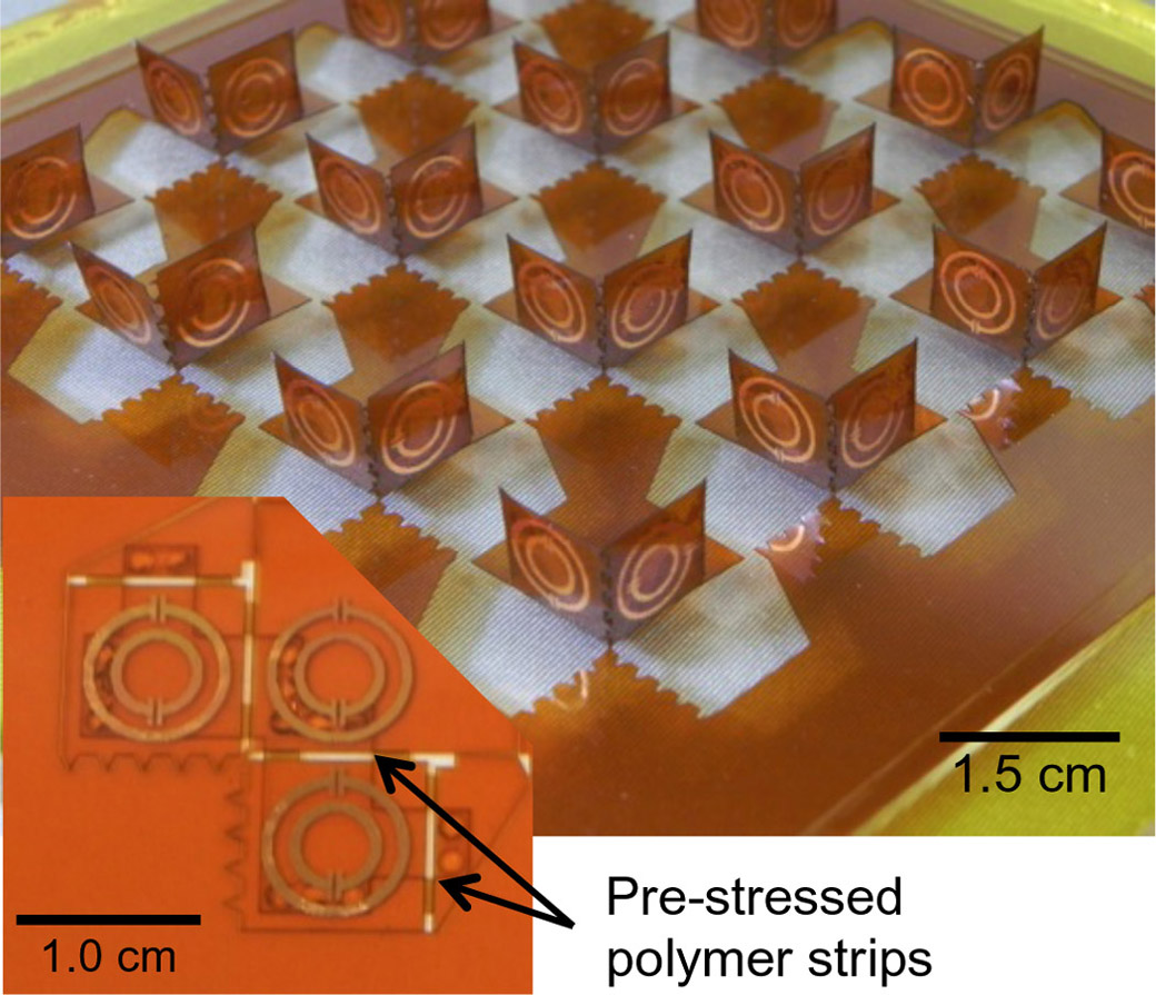
Finally, we have attached laser-patterned prestressed polymer strips across the hinges to create folding 3D assemblies, where the polymer's heat-induced shrinkage provides the actuation mechanism. Figure 4 shows an example of such a 3D structure, in a prototypical split-ring resonator array with resonators along each of the three axes. As in this array, laser origami can fabricate 3D structures with dimensions that are subwavelength for a large portion of the electromagnetic spectrum. These types of structures are the constituents of artificial materials with novel electromagnetic properties known as metamaterials.
Laser origami has the potential to be applied to the fabrication of foldable structures comprising electronic and optical components for highly integrated electro-optic systems. Alternatively, it can be applied to the production of artificial electromagnetic materials over very large areas using roll-to-roll processes. These are just some examples of the kinds of opportunities that laser origami process has to offer. Time will tell how other applications might benefit from this new technique.
In summary, laser origami is uniquely suited to provide engineering solutions for the fabrication of novel folded out-of-plane structures incorporating patterned foils as well as 3D constructs incorporating electronic and/or optical devices. The technique addresses many of the major limitations of current processes such as lithography, namely, processing of large-area and multiscale structures of dissimilar materials and plastic substrates. A different approach is also taken with respect to the actuating mechanism, which is based on strain generation through various types of processes such as mechanical deformation, nanoparticle sintering, and shrinkage of prestressed polymers. In future work, we will investigate the assembly of ‘bricks’ from stacks of folded arrays to generate complex and functionally dense 3D blocks and develop ways to interconnect individual elements within these blocks.
This work was sponsored by the Office of Naval Research.