LCD and Litho Challenge
Liquid-crystal image generation was conceived and realized by RCA in the 1960s. Nearly a decade later, the development of liquid crystal display (LCD) technology led to the manufacture of such products as wrist watches and pocket calculators. In the 1980s, thanks to the commercialization of twisted-nematic (TN) and super twisted-nematic (STN) LCDs, the first notebook computers with LCD screens became widely available.
Since then, intense research, development, and production have led to the emergence of thin-film-transistor liquid crystal display (TFT-LCD) as one of the leading flat panel display technologies, competing with plasma display panels (PDP), organic light emitting diode (OLED) displays, and field emission displays (FED), to name a few. A wide range of applications of TFT-LCD has been developed and commercialized, including notebook and desktop PCs, video camcorders, cameras, televisions, and public displays, creating a multibillion-dollar industry (global panel production value1 of more than US $68 billion in 2007).
With the growth of the industry, vertical integration of local and global TFT-LCD supply chains (mainly located in the Pacific Rim) became more pronounced, starting in Japan, Korea, and now Taiwan. Consequently, the entry barriers for businesses steadily rose.
Despite the aggressive growth worldwide, the TFT-LCD industry is still at a moderate distance from saturation and maturity. As is described in a June 2007 Morgan Stanley Research report2 on global TFT-LCD, the TV display market, using the current leading application for LCD technology, is only half way through its potential penetration.
And the pressure is on to build even larger manufacturing facilities to produce larger TV displays of 50" and beyond.
As in the manufacture of integrated circuits, photolithographic manufacture of displays has challenges to overcome to achieve large-scale production that drives down price. The TFT-LCD industry is wrestling with uniformity, thermal, and critical dimension issues as it attempts to fabricate even larger displays. And these are only a fraction of a long list of challenges and opportunities for the research, development, and commercial manufacturing of the exponentially growing TFT-LCD industry.
Scientists in this exciting field are addressing the challenges through the engineering of materials, electronics, chemistry, equipment, processing, and metrology. The examples presented below are a general and brief preview of Wen-yi Lin's plenary session at SPIE Lithography Asia, to be held in Taipei, Taiwan, in November 2008.
Figure 1 illustrates the strong influence of TV applications on glass substrate size and the generation of fab facilities and technologies. But, what are the challenges encountered by process and equipment technologies to meet the increasingly rigorous requirements of thin-film-transistor array production on a state-of-the-art Generation 8.5 (Gen 8.5) mother glass (2.2 x 2.5 m) with microscopic precision, compared to the requirements in advanced semiconductor IC processing?
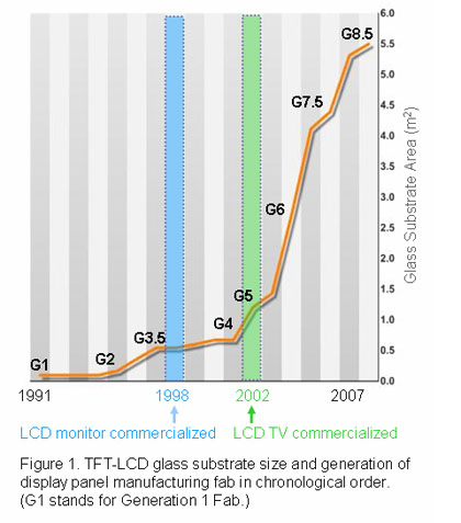
It is well known that TFT-LCD manufacturing utilizes clean-room processing similar to semiconductor production. However, unlike IC, whose critical dimension is being driven down to nanoscale (32 nm) to increase computing speed and reduce cost, TFT-LCD technology development focuses on materials, equipment, and processing engineering of critical-to-quality "uniformity" throughout the entire display, while maintaining a transistor channel length in the range of 2-4 microns.
Additionally, modern IC technology is being developed to confront 45-cm wafers, while a state-of-the-art Generation 10 TFT-LCD fab (substrate size: 285 x 305 cm) is being constructed to produce 65-inch flat panel display.
This comparison indicates that there is clearly a different set of technical challenges to the commercial advancement of the TFT-LCD industry, and this is an area that is attracting tremendous R&D and production interest.
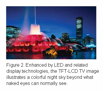
As with size expansion, the advancement of today's display picture quality and performance, coupled with high definition digital broadcasting and/or blue ray DVD signals, has brought crystal-clear, vivid picture quality that human eyes had never experienced in the past.
Figure 2 is an example of how technologies can help the naked eye see a colorful but dark night sky. This is made possible with the improved capability of LED-LCD TV with stringent specifications (Full HD at 1920 x 1080, contrast ratio of 8000 to 1, frame rate of 120-180 Hz, and color saturation at NTSC 92%, cold cathode fluorescence lamp-base, NTSC 120%, LED-base). To get this kind of clarity, it is imperative to have precise control of key photolithography parameters and other processing factors.
Just as semiconductor chips produced on a single wafer might perform differently (clock speed), TFT-LCD with "sufficiently" different electronic and chemical behaviors in local areas can exhibit mura, a Japanese term describing non-uniformity, on the final display. Many factors such as critical dimension, metal line conductivity, and parasitic capacitance-all of which are familiar to people in the IC fields-contribute to mura.
In comparison, TFT-LCD-exclusive concerns are, for example, differential overlay of critical functional structures and total pitch control (a measurement of both microscopic and macroscopic dimension match of color filter and TFT array glass substrates of a display panel). Though human eyes have a very limited spatial resolution, on the order of one tenth of a millimeter, they are extremely sensitive to minute, gradual change (particularly, in orderly fashion) of local non-uniformity, as shown in Figure 3.
In physics terms, the changes of differential overlay contribute to deviation of parasitic capacitance coupled between, say, data lines and their nearby pixels, interfering pixel voltage charging ratio. Consequently, this alters the liquid crystal orientation/alignment of the affected pixels, compared to those in the vicinity, resulting in display mura. Equipment, processing, design, and metrology are now being investigated to improve the monitoring and control over the process.

As glass substrates used for TFT-LCD applications are produced through rapid quenching from its molten state (greater than 1000°C) to room temperature in minutes (in the case of fusion flow production process), they are in a metastable state. This results in the tendency of the substrate to irreversibly shrink as a function of temperature and time during subsequent thermal exposure, necessary for TFT-LCD processing.
For example, the irreversible thermal shrinkage of a Gen 8.5 glass is on the order of several microns diagonally, after LCD processing. Beside the aforementioned phenomenon, reversible thermal expansion of nearly 1000 microns (in diagonal) of Gen 8.5 glass per 1°C change can be observed.
Because an LCD panel is a sandwich of TFT and color filter glass sheets, each with its own distinctive thermal treatment history after their production processing, it is critical to effectively control both the irreversible and reversible thermal expansion. Otherwise, poor total pitch control will frequently lead to TFT-color filter glass dimension disparity and we would see partial light leakage through supposedly "dark" matrix or lines. The slight perception of gray level change again results in mura. Work to address these thermal issues includes process and metrology control.
Another unique challenge for TFT-LCD production includes color filter resist materials and processing to achieve higher color contrast and color saturation. Our recent unpublished study3 showed that 2008 year-end color filter resist contrast (purely material effects) was expected to have a 4-fold increase from its 2004 counterparts. The improvement of color contrast and saturation has mainly been achieved through reducing pigment particle size and increasing its concentration, respectively.
However, as pigment size decreased, more dispersion agent was needed to maintain uniform pigment distribution in the resist. The combined effects, in turn, led to a lower ratio of other essential color resist constituents, namely photo initiators and resin (mainly polymer and monomer). A reduced quantity of resin would challenge the process window of photo exposure and development, potentially leading to, for example, undesired rugged pattern profile at pixel fringes or lower adhesion of resist to glass substrates.
The balance and control of these trade-offs and improvement of dispersion technology are of great interest to those skilled in this art.
During resist deposition, non-uniform thickness of resist coating has often been observed around the edge of the underlying structure. The uneven over-coating (tsuno) lessened optical contrast because it disturbed the alignment of liquid crystal under electric field operation, displaying incorrect gray level to the human eye.
Therefore, it is extremely important to reduce tsuno. This can be accomplished by applying another top coating to average out the non-uniformity or reducing the underlayer's thickness. A combination of equipment, materials, and processing innovations are being engaged to deal with this issue.
1. "Monthly Sales Revenue Tracker_June 2008," WitsView.com, July 17, 2008.
2. F.A.Y. Wang, M. Ono, S. Kim, K. Han, and S. Gupta, "Global TFT-LCD," Morgan Stanley Research, June 21, 2007.
3. W.-B. Wu, unpublished work, 2008.
Authors Wen-yi Lin, Wen-Bin Wu, J.T. Chang, Meng-Ta Tsai, and Wen-ti Lin work for AU Optronics Corp. (www.auo.com) in Taichung, Taiwan.
 Wen-yi Lin, director of L6A Fab, the main TV manufacturing facility at AU Optronics, will give a plenary talk at the SPIE Lithography Asia Symposium in Taiwan on 4 November. Lin will discuss advancements in the engineering of materials, electronics, chemistry, equipment, processing, and metrology for the exponentially growing TFT-LCD market. His talk is titled, "Recent advancements and future challenges of photolithography of TFT-LCD for display applications.
Lin received his PhD from the School of Materials Science and Engineering at Georgia Institute of Technology (USA). He has 14 U.S. patents, numerous equivalent international patents, and 20 publications.
His L6A fab is the leader in the Lean Production and Assistant Engineers Systems in AUO. In addition, he chairs the Thin Film Technology across fab committee at AUO.
Have a question or comment about SPIE Professional magazine? Write to us at spieprofessional@spie.org.
Posted October 2008


