March of the Metamaterials
It's interesting to see how technology evolves. Over the past 20 years or so, diffractive optics, thin films, and photonic crystals have all come and gone as fashionable elements for manipulating light. All of these are kinds of nanotechnology (even though they were around before the term itself became so fashionable) and all manipulate radiation using sub-wavelength features. In addition, all exploit the raw material properties of individual fringes, films, or planes--usually optical density or refractive index--in order to create an optical effect.
However superficially similar, metamaterials are conceptually very different. The idea is not to exploit the underlying properties of the chemicals used (though they're crucial in material design), but rather to create completely new material properties. This is done by creating structures that respond to the incoming radiation actively rather than passively, setting up some kind of oscillation or field that then changes how the light propagates through it.
A classic example of such a material is the split-ring resonator structure (Figure 1 below) developed by David Smith and his colleagues (then at the University of California, San Diego, now at Duke University, NC).
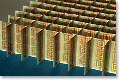
Figure 1: This material, designed by David Smith, has a negative refractive index at microwave frequencies.
Two concentric copper circles with splits in the top of one and the bottom of the other constitute the active element of this structure. As radiation (in this case, in the microwave band) propagates through, energy is picked up by electrons in the metal that then circulate and cause a current to flow. At the same time, the gap in the circle creates a capacitance producing a resonating field that affects the microwave propagation. The result is that the material has a negative magnetic permeability and electrical permittivity, and so a negative refractive index.
Since none of the constituents have this property on their own -- nor, for that matter, do any other elements, compounds, or crystals found in nature?this is a true metamaterial.
In optics, negative refractive index is an extremely interesting property. It literally means that light entering a denser medium bends in the opposite direction to the positive direction we're used to (see Figure 2). Forty years ago, Victor Veselago showed that, if such a material could be created, it could be used to build a completely flat lens that would nevertheless focus light.
However, it took Imperial College theoretical physicist Sir John Pendry to figure out that such a lens could not only focus, but focus beyond the diffraction limit; unlike in positive-index lenses, high-frequency features are not lost to evanescent waves.
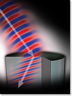
Figure 2: Artist's rendering of a negative refraction in a new semiconductor metamaterial developed at Princeton. (Figure by Kevin Bullis)
Because of its revolutionary nature, Pendry's discovery took a long time to receive acceptance, even from his Imperial colleagues. He says, "When I had the idea that the Veselago lens could be perfect, given the right choice of parameters, I naturally turned to Chris Dainty who is famous for his work on classical optics. I wanted some straight criticism and knew that Chris would not pull his punches.
"As expected, his first reaction was extreme skepticism. But as we worked through his objections, it became clear that if my theory was wrong, it was for subtle and interesting reasons. In fact, it is correct for subtle and interesting reasons!"
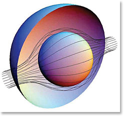
Figure 3: One way of cloaking an object is to make light flow around it like a stream of water, a function that can be performed using a negative refractive index material.
His collaborator David Smith, by this time at Duke, implemented his device for microwaves with impressive -- and now well-known -- results (Figure 4).
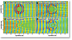
However, the cloak shares a problem with all metamaterials: Its properties are frequency dependent. This means that one designed to work at microwave frequencies will not be cloaked in the visible or RF, and will be poorly cloaked at some frequencies within the microwave band. Worse, a recent study by Zhichao Ruan and his colleagues at the Royal Institute of Technology in Sweden and Zhejiang University in China says that the ideal cylindrical cloak -- if it could be implemented -- would be sensitive to even tiny perturbations. Nevertheless, the concept has attracted significant attention so aided development in the field as a whole.
A useful version of Pendry's perfect lens is also far away -- at least at optical wavelengths. It has proven difficult to find materials with the same properties in, for instance, the visible as are available for lower frequencies.
Still, there have already been developments in better-than-diffraction-limited imaging that use metamaterials.
Take the demonstration reported in 2007 by Zhaowei Liu, Xiang Zhang, and others at the National Science Foundation Nanoscale Science and Engineering Center at the University of California, Berkeley. Based on earlier work done by theorists in the field, they built a so-called hyperlens (see Figure 5) that can be used to image a sample in contact with a cylindrical cavity in the lens itself.
The system is illuminated from the top and the light propagates through a cylindrical metamaterial structure that has a magnetic permittivity in the radial direction opposite that in the tangential direction. As a result, the evanescent wave is pulled into the lens, the image is magnified as the light propagates through it, and the larger image can be read by a conventional lens.

According to Zhang, their first hyperlens was designed to work at ultraviolet wavelengths because it was easy to do so. "It is possible to use it as a tool for research," he says, "but it's not quite ready for general applications, especially for imaging living cells. We are working on developing a visible hyperlens for that."
This is easier said than done, admits Zhang. "Theoretically, the biggest obstacle [to progress] is the inevitable loss in the metamaterials. This means that -- to obtain reasonable transmission -- the hyperlens can't be very bulky; this will limit the magnification and imaging area …. Low loss metals and high refractive index dielectrics will greatly boost this field but are extremely hard to find."
Pendry agrees that loss is a major issue for optical metamaterials. "Typically we might use highly conducting metals such as copper or silver which work just fine until we try to use them at the highest frequencies where they become lossy. We need the help of materials scientists to develop new alloys with lower losses."
That said, metamaterials approaching optical frequencies have been proven possible.
Researchers at the University of Karlsruhe have published details of a three-layer negative index material that operates around 1.4 µm. Here, two layers of crossed silver wires are used to create the desired effect. Oscillations created by the light passing through produce both negative permeability and permittivity, the classic conditions required to create a negative refractive index. However, though initial results have been positive, researchers are not sure their structure will work as well in optically thicker media. "… It is still a long way to truly three-dimensional isotropic negative-index metamaterials at optical frequencies," G. Dolling and colleagues reported in Optics Letters in March 2007.
Another approach being taken by many researchers is to use plasmonics. Anatoly Zayats, a researcher at the Centre for Nanostructured Media at the Queen's University of Belfast in the UK, explains that in the visible and near-infrared frequency ranges, the optical properties of the kind of metallic nanostructures that researchers have been looking at "are completely determined by one or another type (or several types) of plasmonic excitation such as surface plasmon polariton, localized surface plasmon, particle plasmon, etc. The coupling of light to plasmonic excitations that are collective electronic excitations in metallic nanostructures allows one to confine the electromagnetic field on the sub-wavelength scale and manipulate it with high precision. Both these properties are difficult to achieve with dielectric metamaterials."
Nevertheless, it seems that such properties have been achieved. Not quite at optical frequencies, but long-wave infrared. At the end of 2007, Princeton researchers reported they had developed an optically-thick low-loss negative-index material consisting of alternating layers of highly doped InGaAs and AlInAs -- no metals. Interestingly, the Princeton material uses an entirely different effect than the others to implement the negative index. The optical properties are created by anisotropy in the material's dielectric response rather than resonances in both the permeability and permittivity of the constituent layers. This gives it an inherent flexibility.
On top of its other advantages, the Princeton metamaterial is the first in a new class not only in terms of mechanism but in its potential to be practically fabricated. Anthony Hoffman, the graduate student who has been developing the material based on work done by Evegenii Narimanov (now at Purdue University) quotes his doctoral adviser, Claire Gmachl, on this. She puts it succinctly: "Semiconductors are the things from which true applications are made."
Given the massive investment in the semiconductor industry, it's hard to argue with that.


