Bubble and antibubble defects in 193i lithography
The difference between 193nm immersion lithography and conventional photolithography is that, in the former, water fills the space between the front lens and the wafer. Replacing air with water enhances the depth of focus and enables the numerical aperture (NA) to be increased to values greater than 1.1 However, physical and chemical interactions can occur between the water and the resist/topcoat stack. This leads to immersion-related defects, of which the major types are bubble and `anti-bubble’ types, as well as water marks, particles, and microbridges.2–4 These are observed on almost all 193nm immersion-processed wafers and account for more than 90% of the total defects. This article describes these bubble and anti-bubble defects—other kinds are discussed in a later article.
Bubble defectsAir in the immersion water causes bubbles: an air bubble reflects or refracts the exposure light and thereby distorts the local image projected on the resist. Usually, bubble defects are circular and have diameters ranging from one to several hundred micrometers. The impact of bubbles on the image depends on their size and distance from the resist surface. It is generally accepted from various theoretical and experimental results5,6 that free-floating air bubbles in the water have less impact because they are out of the imaging focus. Furthermore, floating bubbles have very short lifetimes.7 The real threat comes from those attached to the surface.
An air bubble on the resist surface works like a small lens during exposure: it diverges the exposure light and distorts the pattern underneath and around itself (see Figure 1). After development, the distorted pattern forms a circular defect. The effects of bubbles on imaging were simulated by several different groups.5,6,8 In particular, work by Peter De Bisschop, Andreas Erdmann, and Andreas Rathsfeld helps us to recognize bubble defects and differentiate them from other circular defects in experiments.8 According to their simulations, the most noticeable effect caused by a bubble is the strong reduction in image intensity at the bubble location on the resist surface, whereas at certain locations around the bubble the image intensity increases. The bubble also seems to magnify the incident line and space pattern.

Figure 2(a) shows a typical bubble defect on a line and space pattern. It is circular, with a diameter of about 9μm. As predicted by the simulation, the bubble causes under-exposure in the local area. In the central region of the defect, image modulation is visible, but the pattern is magnified. The pitch of the pattern is 220nm in the well-patterned area as designed; however, in center of the defect, it is measured as ∼308nm. The magnification ratio is ∼1.4. Moving from the center to the edge, the imaging modulation gets weaker and weaker, finally completely disappearing at the edge of the bubble.

In general, the area that surrounds the bubble defect is over-exposed. Looking closely, we can observe intensity fringes in this area. Figure 2(b) shows an amplified scanning electron microscope (SEM) image taken at the edge of another bubble defect. In the surrounding area, the resist is completely developed, making the edge of the bubble defect very sharp and clear. A little away from the edge, resist lines appear, which indicates a lower local dose. Further away, the resist lines gets thinner—as though pinched—indicating a higher local dose. The variation in resist linewidth shows spatial periodic behavior corresponding to the dose modulation. Further away from the defect, the dose modulation weakens and finally becomes imperceptible. Figure 2(c) shows a low-magnification SEM image. The fringe pattern caused by the dose modulation can be better observed outside of the bubble defect. Obviously, the dose modulation derives from exposure light reflection and refraction by the bubble.
From our experience with defect inspection, we find that big bubble defects with diameters greater than 2μm are relatively easy to identify. One or more of the features described above are usually visible. The imaging modulation is clear, leaving ample information on the resist pattern. This is because reflection and refraction of the exposure light by a big bubble is stronger than that of a small bubble. The challenge is to identify small bubble defects for which the features described in previous paragraphs are not clearly visible. For example, a defect caused by a roughly 100nm-diameter bubble may look just like a small bridge connecting two resist lines.
The source of bubbles in immersion water is still under investigation. It seems that they are most likely trapped by a non-optimized exposure head design.9 Also, surface topography has proven to have minor effects on bubble formation.10 Therefore, better exposure head design appears to be the key to reducing these defects. Recognizing this, scanner vendors have produced new designs and now claim ‘no bubble’ processes.11,12 Complete degassing of the immersion water and use of low outgassing resists are helpful for further reducing bubbles.
Anti-bubble defectsThe ‘microlens effect’ can also be caused by a transparent particle or bump, for example, formed by topcoat particles. Figure 3(a) shows a diagram of a spherical topcoat particle attached to the surface. The refractive index of the topcoat is ∼1.55, which is larger than that of water. The transparent particle focuses the exposure light (the opposite effect to that of an air bubble). The center area underneath the particle tends to get overexposed, as indicated by the gray scale in Figure 3(b). Near the edge of the particle, the exposure light is mostly reflected due to the high incident angle at the interface of water and particle. A heavily underexposed ring is expected at the edge of anti-bubble defects. This was first observed in a deep-UV-processed wafer. It was attributed to the resist particles.13

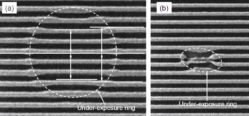
Figure 4(a) shows a SEM image of an anti-bubble defect. It is circular, with a diameter of about 1.7μm. As predicted, we observe the underexposed ring surrounding the defect. In the center of the defect the resist lines are slightly narrower than near the edge, which indicates convergence of the exposure light. The resist lines in this area shift towards the center, and their pitch is smaller than in the unaffected area. This is due to the demagnifying effect of the particle `lens'. The shape of the particle defines the extent of the demagnification effect. A particle with high curvature generates a more pronounced demagnification effect and underexposure ring. Figure 4(b) shows another anti-bubble defect. Although it is smaller than that in Figure 4(a), the pattern demagnification and under-exposure ring are very pronounced. The two resist lines in the defect area are hardly resolved. As suggested by Figure 4(b), the shapes of anti-bubble defects are not necessary perfect circles. They can also be oval.
The source of the transparent particles is attributed mainly to the topcoat material and a non-optimized coating process. After the topcoat solution is stored for a long time, chemical segregations can generate particles and clusters. When these are delivered to the wafer surface, they form bumps embedded in the topcoat film. During the coating process, excessive topcoat or resist spins off the wafer and lands on the wall of the coating bowl. The topcoat sticking to the wall dries and forms particles. In the next wafer process, the high spin speed will create a vacuum on the wafer surface and suck at the particles.
Water uptake has been demonstrated as another way to form bumps in the resist and topcoat.14 Due to surface imperfections—for example, the existence of pinholes—water may penetrate through the topcoat and reach the interface between it and the resist. The water swells the topcoat film and forms circular bumps. Filtering the topcoat solution before applying it to the wafer surface and cleaning the coating bowl frequently have proven to effectively reduce anti-bubble defects. Improving the coating uniformity also helps to reduce defect counts.
Bubble defects are unique to the immersion process, while anti-bubble defects are also observed on dry-processed wafers, but the immersion process provides additional sources of particles. The mechanism by which immersion-related defects are formed may involve the scanner, the materials (including bottom anti-reflection coating, resist, and topcoat), and the process setup. The defects we addressed are introduced by the scanner.
The author thanks Dr. Stefan Brandl of Qimonda AG for his collaboration.


