High-throughput fabrication of planar chiral metamaterials
Recently, planar chiral metamaterials (PCMs) have emerged as a promising new material and attracted research attention worldwide.1 PCMs' elements are chiral (or ‘handed’) because they have no line of symmetry in the plane of the structure. Consequently, PCMs interact differently with left- and right-hand polarized light, which has great significance for chemical and biological sensing applications. For example, a PCM has been used to detect picogram-level biomolecules exhibiting chiral planar sheet structures, indicating potential applications for detecting important diseases such as Alzheimer's.2Until now it has been necessary to use precision nanotechniques to fabricate PCMs, but the high cost and low throughput of this hinders commercial applications. As a result, there is great interest in developing low-cost, large-scale fabrication methods. Nanospherical-lens lithography (NLL) is an economical fabrication technique that is capable of producing large-area arrays of nanoscale disks. It uses polystyrene nanospheres as lenses to focus incoming UV light on an underlying photoresist layer in arrays of dots, which on developing form arrays of holes in the photoresist. A subsequent process of metal evaporation and lifting-off forms the metal nanodisk arrays. Our research group is regularly fabricating arrays of nanodisks, covering an area as large as 1cm2 with nanodisk diameter of less than 100nm.3, 4
 Colleagues and I have recently begun to fabricate nano-ellipse arrays by replacing the light source with a commercial UV lamp.5 UV light from the lamp propagates and focuses differently perpendicular and parallel to the lamp. Figure 1 shows the simulated time-average field energy distribution near a polystyrene nanosphere when illuminated with a line-shaped UV light source (wavelength 365nm) oriented parallel to the y-axis. Simulation was done by the 3D finite-difference time domain method. Comparing Figure 1(a) and (b) reveals that the propagation of the incident light across the xz- and yz-planes clearly demonstrates different behaviors and focusing spot sizes. Figure 1(c) shows the distribution across the z=1μm plane, marked as dotted white lines in Figure 1(a) and (b). The distribution reveals an elliptical pattern and explains why elliptical photoresist holes form. The long axis of the nano-ellipse is always parallel to the lamp direction, giving control of the orientation of the nano-ellipses. We have also discovered that localized surface plasmon resonance (LSPR) of the nano-ellipse arrays, whose long-axis length exceeds 1μm, is in the IR region. Consequently, the nano-ellipse arrays can be used as platforms for surface-enhanced IR absorption.5

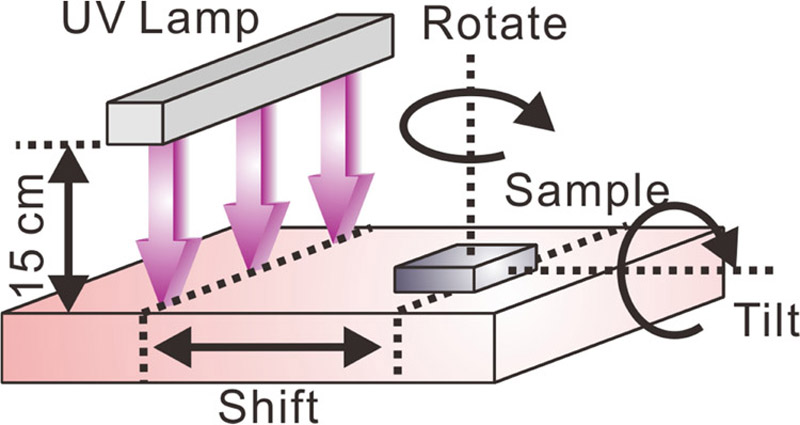
We can also vary several exposure parameters, including the exposure duration, the angle between exposures, the sample location, and the tilt angle of the sample (see Figure 2). By careful design of the exposure sequence, we can make different nanostructures: see Figure 3(a–o). For example, if we rotate the sample for 60° and perform the second exposure, we can fabricate the butterfly-shaped pattern shown in Figure 3(b). We can also design the exposure sequence to fabricate the L- and Z-shaped patterns shown in Figure 3(j) and (l) and their mirror images shown in Figure 3(k) and (m). This is achieved by rotating the sample either clockwise or counterclockwise before exposure. These patterns possess no line of symmetry in the plane of the structure and can be recognized as PCMs. The tilt angle of the sample during the exposure is also another degree of freedom that we can change, which will result in two parallel nano-ellipses with an offset center located along one direction: see Figure 3(n) and (o). The shift distance is found to be larger with increasing tilt angle. The pair of such nano-ellipses can also be recognized as PCMs.

In conclusion, we have demonstrated the fabrication of PCMs by NLL using a commercial UV lamp as the light source. The fabrication is high-throughput, and the fabricated arrays cover a large area, which should help the fabricated PCMs to find practical application in devices that selectively reflect and transmit different polarization states. These would be useful for chemical and biological sensing applications such as detecting diseases like Alzheimer's. In the future, we hope to further reduce the size of each chiral element so that their LSPR response can be in the visible range, which would enable a broader spectrum of applications. Our final goal is to develop some novel applications that require using large-scale PCMs fabricated by this proposed method.
We thank the National Science Council, Taiwan, for financial support under grant NSC 101-2112-M-001-030-MY2. We are also grateful for collaborations with the Center of Micro/Nano Science and Technology, National Cheng Kung University, Tainan, Taiwan, and the National Center for High-Performance Computing of Taiwan.
Academia Sinica
Taipei, Taiwan
Yun-Chorng Chang is an associate research fellow whose research interests focus on developing various nanofabrication techniques and how to apply them in the fields of nanophotonics and biosensing.