Imaging visible and IR light
By placing quantum dots on top of graphene, a highly sensitive photodetector is constructed that works simultaneously for visible and IR light.
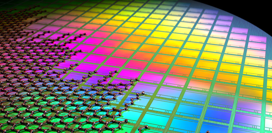
Flagship researchers from ICFO integrate graphene and quantum dots with CMOS technology to create an array of photodetectors, producing a high resolution image sensor. Courtesy Fabien Vialla.
Human vision is only capable of converting a tiny fraction of light into an image. Although our eyes can see visible light, they are completely blind to 99% of the infrared light, a range of light that our bodies can only perceive as heat.
The imaging technologies we commonly use to capture images, such as digital cameras, are not able to do any better than human eyes. This is to some extent a coincidence, but can be explained by the fact that most common imaging systems are based on silicon chips, which use silicon electronic integrated circuits and silicon photodetectors. These silicon photodetectors can only convert visible light into electrical signals.
Integrating non-silicon semiconductors for IR light into imaging systems is a challenging process since these types of semiconductors perform poorly when combined with manufactured circuits based on the well-established Si-CMOS technology circuits. This limitation has resulted in IR imaging sensors costing as much as three orders of magnitude more than visible-wavelength Si-based image sensors, not to mention that they also have limited pixel resolution.
Photodetector ‘sees' IR light
This major drawback has now been overcome, thanks to graphene and semiconducting nanoparticles known as quantum dots. Graphene is an atomically flat material, consisting of a crystalline lattice of carbon atoms, used in this case as an electrical conductor with extraordinary high electronic mobility. Colloidal quantum dots offer high absorption and bandgap tunability from UV to short-wavelength IR.
By placing these quantum dots on top of graphene, a highly sensitive photodetector is constructed that works simultaneously for visible and IR light. These hybrid phototransistors are entirely compatible with silicon technologies, drastically reducing the cost for the development and production of the detection system as well as the electronics.
Equally important is the fact that these detectors can maintain a very high sensitivity while operating at room temperature, despite their spectral coverage into the infrared and unlike IR photodiodes that require cooling to reach compelling sensitivity. Because no cooling is required, the device can be rather slim and lightweight, with low power consumption, features that are essential for applications that require portability, mobility, and seamless integration.
110,000 hybrid photodetectors
At the Institute of Photonics Sciences (ICFO), we have been able, for the first time, to integrate graphene with silicon-integrated circuits in order to build an imaging array of 288 x 388 pixels. This array is considered the most broadband CMOS-monolithic image sensor in the world.
The sensor was fabricated by connecting more than 110,000 graphene-quantum dot photodetectors to the CMOS electronics (containing thousands of transistors) inside a microchip. This configuration permits the conversion of incoming light into electronic signals for each of the pixels, building up an image through their read-out. All this happens automatically and instantaneously inside the chip.

Silicon CMOS wafer with image sensor read-out circuitry, integrated with graphene/quantum dot photodetectors. Courtesy Fabien Vialla
As a result, we obtained the core chip for a digital camera that can sense UV, visible, and IR at the same time.
Since the graphene can be grown on large scale using chemical-vapor deposition and integrated with the CMOS circuitry by a simple transfer technique, this technology is fully compatible with silicon and CMOS technologies, which considerably reduces its production cost.
Optoelectronic applications
The many application areas for this new type of imaging system are highly diverse. First, it can be used as a night-vision camera since the atmosphere at night is always emitting IR light. We cannot see this light with our eyes or with the use of a conventional camera. However, with our newly created graphene-quantum dot camera, it is possible to sense this light and therefore obtain images and videos even when it is pitch black.
Secondly, IR light can propagate through fog, and with the help of this new camera, we can actually "see" objects through it.
Another example could be food inspection. By distinguishing different IR wavelengths, such technology would allow us to see the inside of fruits and vegetables and measure their decomposition state, even before seeing it with your own eyes.
In addition to these safety and security applications, this technology has caught the attention of the automotive, medical imaging, pharmaceutical inspection, and environmental monitoring sectors, and it may bring forward future applications that could include consumer products such as smartphone cameras, wearables, or smart glasses.
The integration of graphene with Si-CMOS electronics is also a promising platform for a broad range of applications, including integrated photonics (for the next generation of data communication infrastructure) and sensor systems (for the Internet-of-Things). For this reason, significant efforts are currently being dedicated to the production of low-cost, high-quality graphene and its integration with silicon CMOS manufacturing lines.
This large-scale integration is one of the main goals of the graphene flagship program, the largest EU research initiative with €1 billion in funding over 10 years. It is expected that wafer-scale production will be ready within a few years, giving support to a bright outlook for the first graphene-based optoelectronic technologies to enter the marketplace.
") -Frank Koppens is an ICREA professor at the Institute of Photonic Sciences (ICFO) in Barcelona where he leads the Quantum Nano-Optoelectronics Research Group. Gerasimos Konstantatos is also an ICREA professor at ICFO and leads the Functional Optoelectronic Nanomaterials Research Group. Stijn Goossens is senior research fellow and project leader. The three are among 16 authors of a 2017 paper published in Nature Photonics, "Broadband image sensor array based on graphene-CMOS integration." Koppens is scheduled to describe this work 30 January at an industry session during SPIE Photonics West.
-Frank Koppens is an ICREA professor at the Institute of Photonic Sciences (ICFO) in Barcelona where he leads the Quantum Nano-Optoelectronics Research Group. Gerasimos Konstantatos is also an ICREA professor at ICFO and leads the Functional Optoelectronic Nanomaterials Research Group. Stijn Goossens is senior research fellow and project leader. The three are among 16 authors of a 2017 paper published in Nature Photonics, "Broadband image sensor array based on graphene-CMOS integration." Koppens is scheduled to describe this work 30 January at an industry session during SPIE Photonics West.
This article was originally published in the January 2018 edition of SPIE Professional magazine.
Related SPIE content:
Frank Koppens: Manipulating light with graphene
With potential uses from photovoltaics to integrated optical circuits, new discoveries can be quickly applied.
Light and graphene
Graphene and other 2D materials may be the basis for the next killer application in optical sensing.
The promise of 2D tunable materials
From the SPIE Photonics West Show Daily: 2D tunable materials would allow researchers to "move from still-life daguerreotype nanophotonics to the film and television era."
Using graphene plasmonics to boost biosensor sensitivity
Plasmonic oscillations on graphene and 2D biocompatible nanomaterials are combined to yield ultrasensitive devices suitable for clinical diagnostics and early treatment of disease.
Superradiant terahertz lasing with graphene metamaterials
Plasmonic dynamics exploit the optical properties of graphene to create a new type of terahertz solid-state laser.
Tuning metamaterials with graphene
Previously challenging spectral blue-shifting of plasmonic metasurfaces is enabled by overlaying them with single-layer graphene, paving the way for next-generation tunable infrared optoelectronic devices.
Graphene for next-generation optical communication
A monolayer of graphene can be used to control the optical absorption in a silicon-based waveguide, inspiring a new category of optical modulators.


